Electron microscope chamber
1344×768 · AVIF · CC BY 4.0
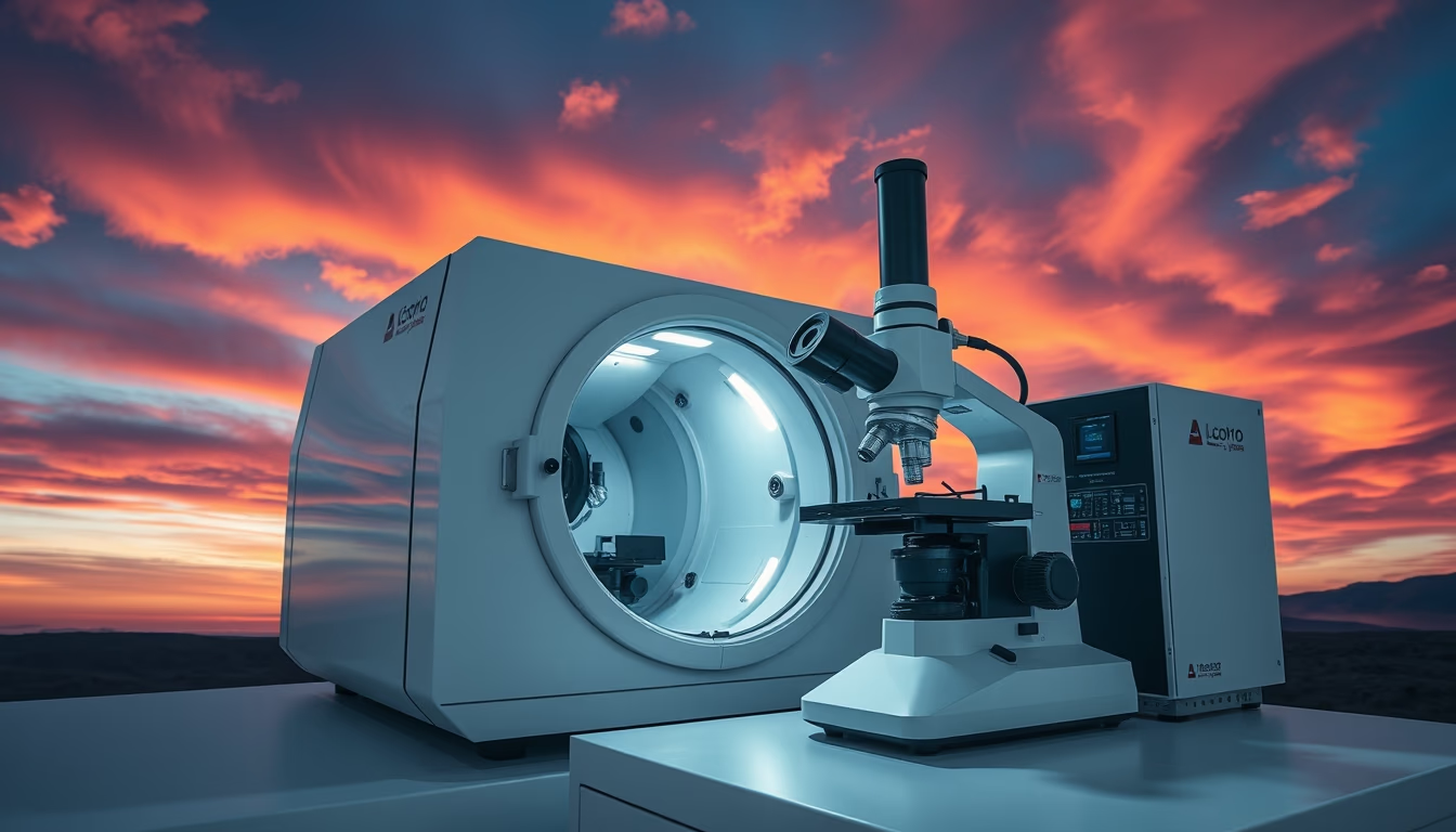
Electron microscope chamber where electron beams generate nanoscale images, essential for materials science and biology research.
About this subject
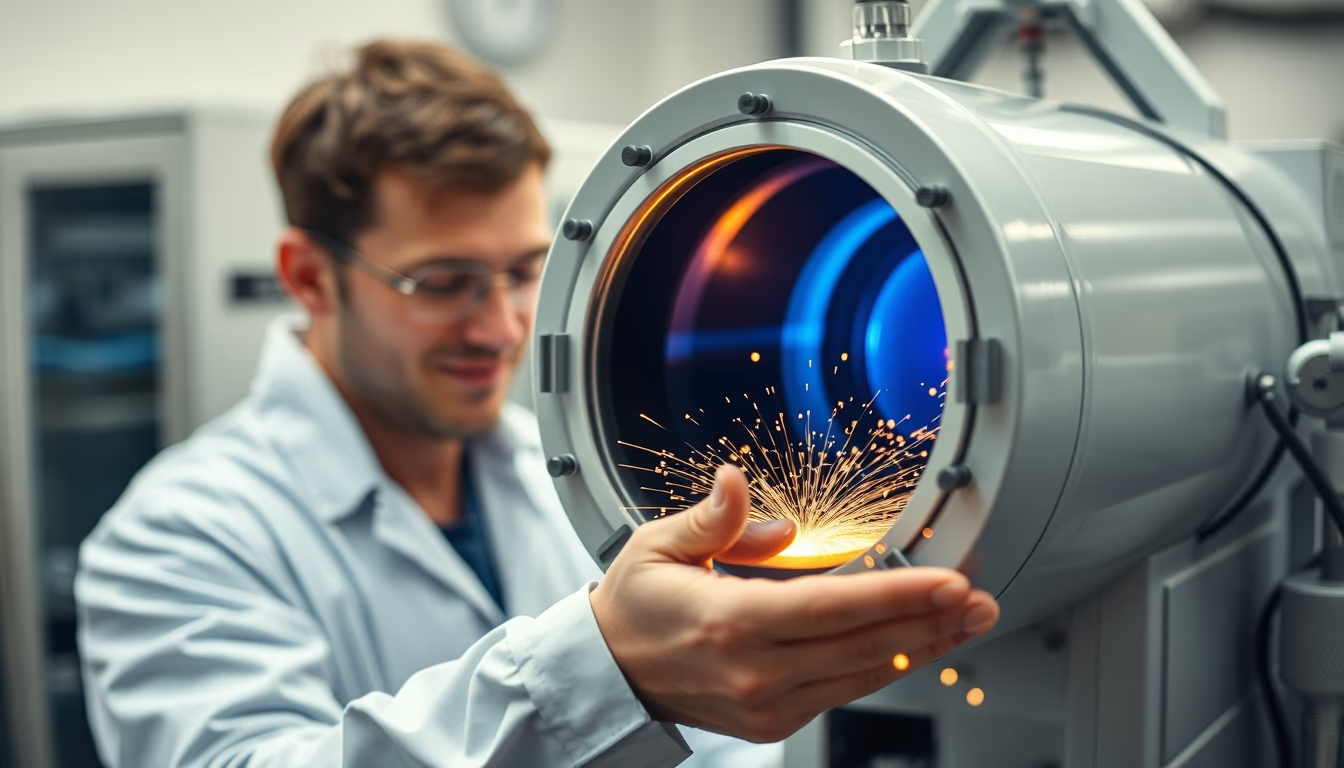
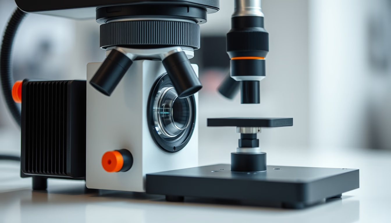
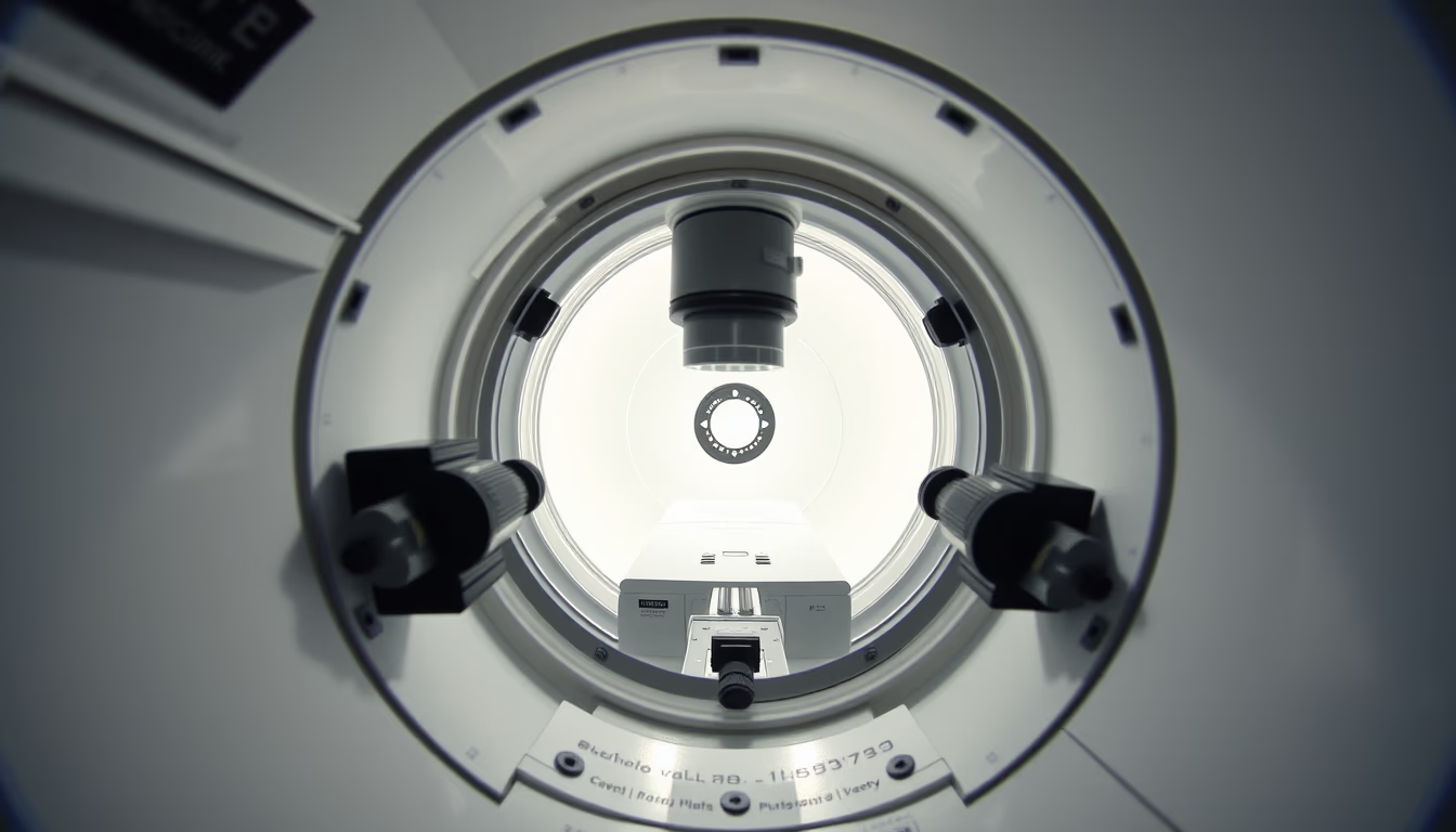
The electron microscope chamber is the central compartment where the electron beam interacts with the sample, producing images with resolution far superior to optical microscopy. This environment operates under vacuum to prevent air molecules from scattering electrons, enabling magnifications up to 10 million times. Inside the chamber, the sample is positioned on a motorized stage with nanometric precision, while detectors capture signals such as secondary electrons, backscattered electrons, or characteristic X-rays.
There are two main types of electron microscopes: scanning electron microscope (SEM) and transmission electron microscope (TEM). In SEM, the beam scans the sample surface, generating three-dimensional topographic images; in TEM, electrons pass through an ultrathin sample, revealing internal details such as crystalline structures. The invention of the electron microscope by Ernst Ruska in the 1930s earned him the Nobel Prize in Physics in 1986, revolutionizing fields like nanotechnology and cell biology.
A technical curiosity is that the long-exposure tag may refer to imaging techniques with prolonged acquisition times, used to improve signal-to-noise ratio in sensitive samples or to obtain elemental maps through X-ray spectroscopy. Modern chambers can also incorporate cryostats to observe materials at cryogenic temperatures, simulating space conditions or low-temperature biological processes.
These instruments are expensive and require specialized facilities, with vacuum pumping systems, high-voltage sources, and cooling. Chamber maintenance is critical, as any contamination can degrade image quality and damage components such as the electron column.
Frequently Asked Questions
What is an electron microscope chamber?
It is the vacuum-sealed compartment where the electron beam interacts with the sample, enabling imaging at atomic and nanoscale resolution.
What is the difference between SEM and TEM?
In SEM, the beam scans the sample surface for 3D topography. In TEM, electrons pass through the sample, revealing internal details and crystal structure.
Why must the chamber be under vacuum?
Vacuum prevents air molecules from scattering the electron beam, ensuring resolution and protecting the filament and sample from damage.
Direct URL
https://pub-c7d6a6ea828543ac903a74a341ccb2e1.r2.dev/imagens/electron-microscope-chamber-long-exposure-fresh15.avifHow to credit
Include a visible link back to UtilizAí. Copy one of the snippets below:
<a href="https://xn--utiliza-eza.com/en/midia/imagens/electron-microscope-chamber-long-exposure-fresh15">Electron microscope chamber</a> by <a href="https://xn--utiliza-eza.com">UtilizAí</a>, licensed under <a href="https://creativecommons.org/licenses/by/4.0/">CC BY 4.0</a>.
[Electron microscope chamber](https://xn--utiliza-eza.com/en/midia/imagens/electron-microscope-chamber-long-exposure-fresh15) by [UtilizAí](https://xn--utiliza-eza.com), CC BY 4.0
License: CC-BY-4.0