Electron microscope chamber
1344×768 · AVIF · CC BY 4.0
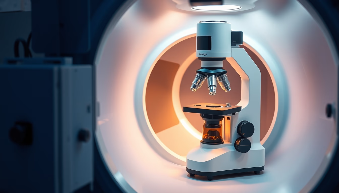
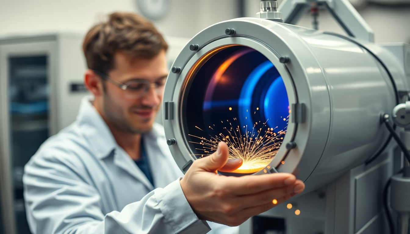
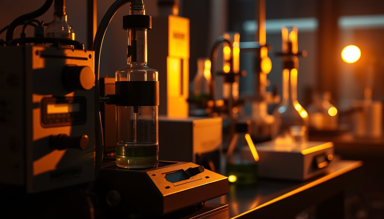
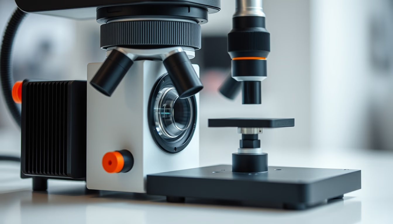
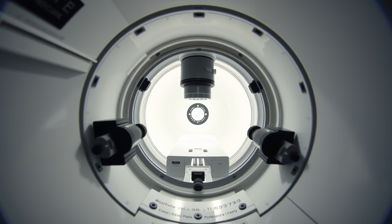
Electron microscope chambers house samples in vacuum and electron beams for magnifications up to 10 million times.
About this subject
The electron microscope chamber is the core component where samples are exposed to electron beams under extreme vacuum conditions. Unlike optical microscopes that use light, electron microscopes employ accelerated electrons, enabling resolution down to individual atoms. The chamber must be hermetically sealed to prevent electron collisions with air molecules, which would scatter the beam and degrade image quality.
Two main types exist: transmission electron microscopes (TEM) and scanning electron microscopes (SEM). In TEM, the chamber allows the beam to pass through an ultra-thin sample, revealing internal structures. In SEM, the beam scans the sample surface, producing high-depth-of-field three-dimensional images. Both chambers include motorized stages for nanometer-precise sample positioning, secondary and backscattered electron detectors, and vacuum systems with turbomolecular and diffusion pumps.
Historically, the first functional electron microscope was built by Ernst Ruska in 1931, earning him the 1986 Nobel Prize in Physics. Since then, chambers have evolved with spherical aberration correctors that enhance resolution and cryo-stages that allow observation of frozen biological samples in near-native states. Vacuum maintenance is critical: typical pressures range from 10^-4 to 10^-7 Pa, depending on application. Modern chambers also support techniques like energy-dispersive X-ray spectroscopy (EDS) for elemental analysis.
Frequently Asked Questions
Why does the electron microscope chamber need vacuum?
Vacuum prevents air molecules from scattering the electron beam, which would degrade resolution and introduce noise. It also protects the filament and extends equipment life.
What is the difference between TEM and SEM chambers?
In TEM, the sample is positioned in a column that allows the beam to pass through it. In SEM, the chamber is larger to accommodate bulkier samples and surface detectors, and the beam scans the sample rather than transmitting through it.
What materials can be analyzed inside an electron microscope chamber?
Virtually any solid, conductive material (or coated) can be analyzed, including metals, ceramics, polymers, and biological samples. Non-conductive samples must be coated with gold or carbon to prevent charge buildup.
Direct URL
https://pub-c7d6a6ea828543ac903a74a341ccb2e1.r2.dev/imagens/electron-microscope-chamber-studio-still-life-fresh14.avifHow to credit
Include a visible link back to UtilizAí. Copy one of the snippets below:
<a href="https://xn--utiliza-eza.com/en/midia/imagens/electron-microscope-chamber-studio-still-life-fresh14">Electron microscope chamber</a> by <a href="https://xn--utiliza-eza.com">UtilizAí</a>, licensed under <a href="https://creativecommons.org/licenses/by/4.0/">CC BY 4.0</a>.
[Electron microscope chamber](https://xn--utiliza-eza.com/en/midia/imagens/electron-microscope-chamber-studio-still-life-fresh14) by [UtilizAí](https://xn--utiliza-eza.com), CC BY 4.0
License: CC-BY-4.0