Electron microscope chamber
1344×768 · AVIF · CC BY 4.0
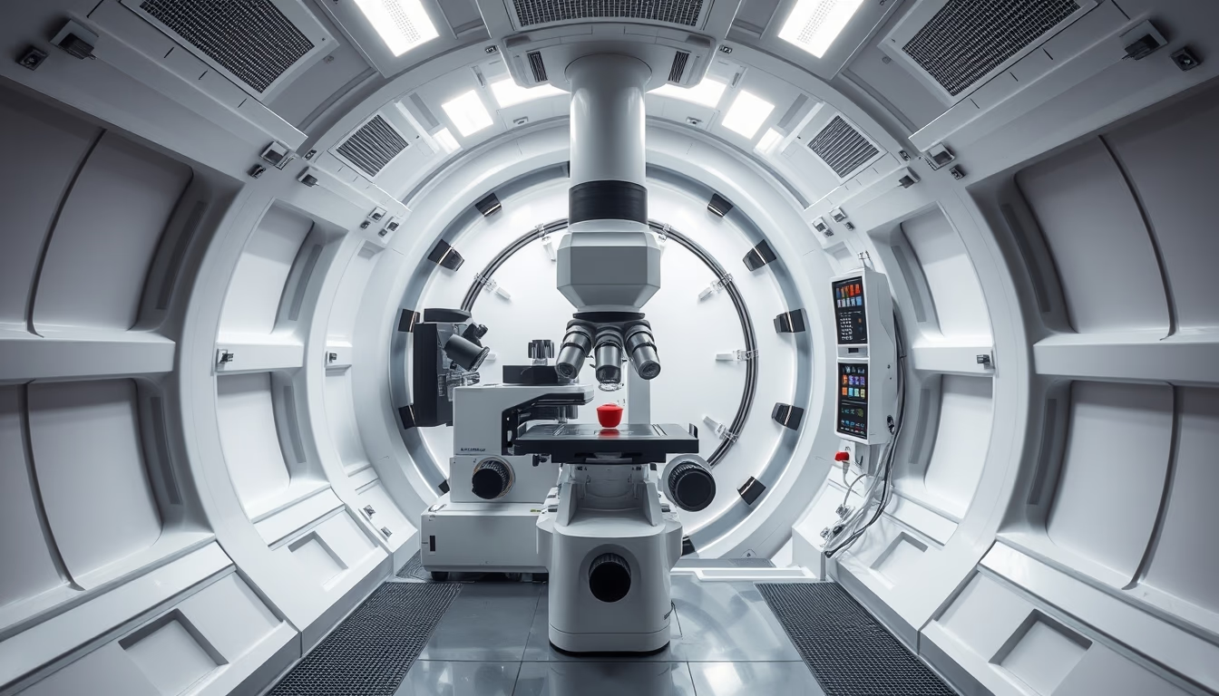
Electron microscope chamber: vital component for magnified visualization of nanoscale structures in materials science and biology.
About this subject
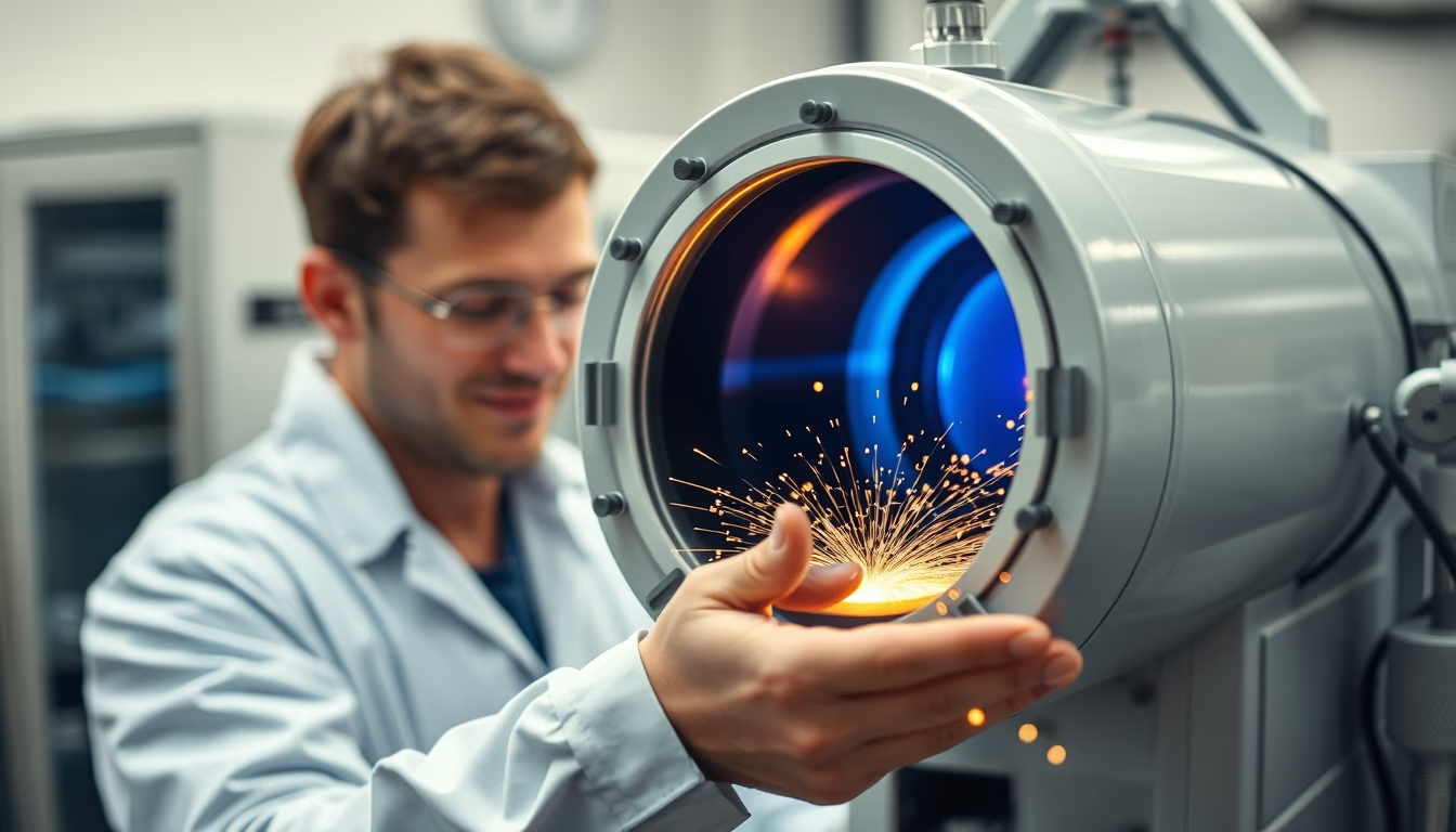
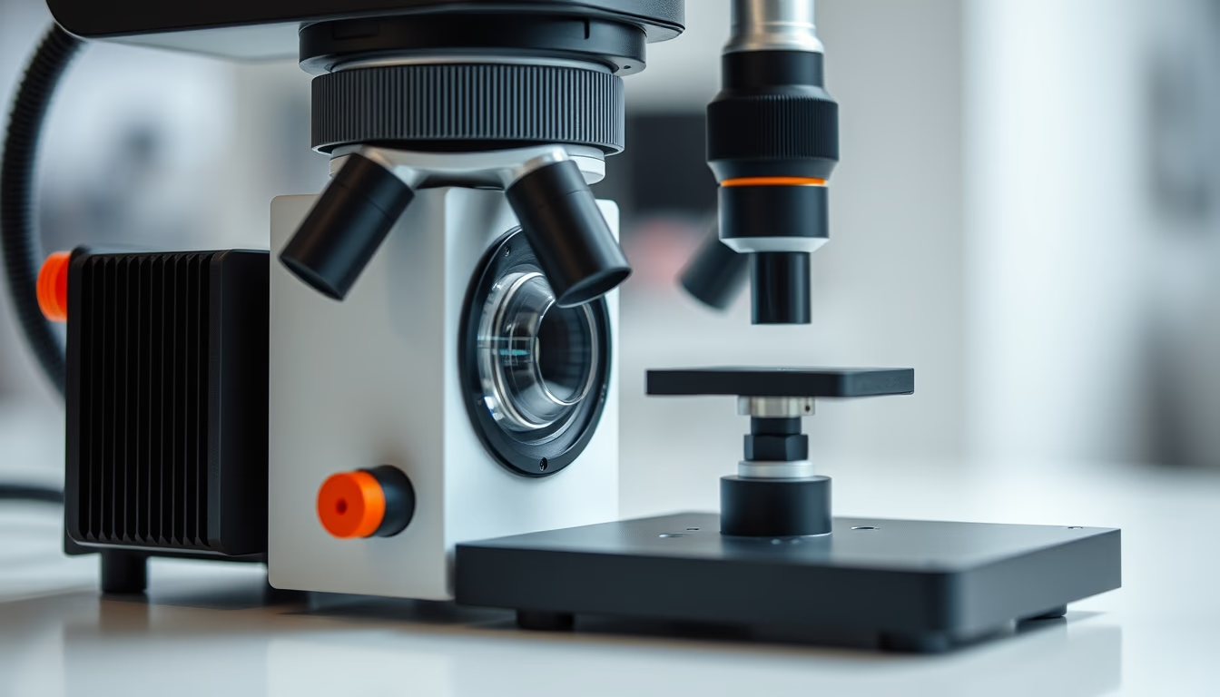
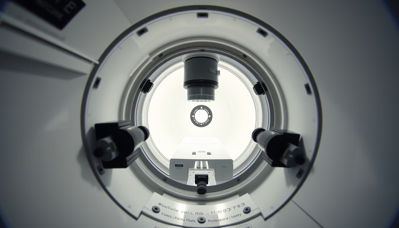
The electron microscope chamber is the central compartment where the sample is positioned and exposed to a beam of electrons. Unlike optical microscopes that use visible light, electron microscopes employ accelerated electrons whose much shorter wavelength allows resolutions on the order of angstroms, enabling the visualization of individual atoms. This technology is fundamental in fields such as nanotechnology, materials science, and cell biology, where ultrastructural details are essential.
The chamber operates under ultra-high vacuum to prevent air molecules from interfering with the electron path. Inside, it contains precise mechanisms for moving the sample in X, Y, and Z axes, as well as rotation and tilt for three-dimensional analyses. The robust design and shielding against external magnetic fields ensure stability during long-term imaging. In scanning electron microscopes (SEMs), the chamber also houses detectors for secondary and backscattered electrons, which form topographical and compositional images.
Historically, the first functional electron microscope was built by Ernst Ruska in 1933, earning him the Nobel Prize in Physics in 1986. Since then, chambers have evolved from simple metal enclosures to sophisticated systems with computer-controlled temperature, pressure, and electric fields. Modern models can achieve magnifications exceeding 10 million times, essential for research on semiconductors, catalysts, and viruses.
Interestingly, many chambers are designed in cylindrical or spherical shapes to withstand external atmospheric pressure while maintaining internal vacuum. Some systems allow the introduction of gases or vapors for in situ studies, such as catalytic reactions or crystal growth. Cleanliness maintenance is critical: dust particles or contamination can degrade image quality and damage sensitive components.
Frequently Asked Questions
What is the difference between the chamber of a scanning electron microscope (SEM) and a transmission electron microscope (TEM)?
In SEM, the chamber is larger and allows broad sample movement for surface imaging, while in TEM the chamber is more compact because an ultrathin sample must be transmitted through the electron beam. TEM requires even stricter vacuum and detectors placed below the chamber.
Why does the chamber require vacuum?
Vacuum is necessary because electrons are easily scattered by air molecules. Without vacuum, the beam would lose focus and energy, and could ionize the air, causing electrical discharges that damage the equipment.
What materials are used to manufacture the chamber?
Stainless steel, aluminum, or special non-magnetic alloys are commonly used. The interior may be coated with materials like gold or carbon to prevent unwanted electron reflections and facilitate cleaning.
Direct URL
https://pub-c7d6a6ea828543ac903a74a341ccb2e1.r2.dev/imagens/electron-microscope-chamber-architectural-photography-fresh11.avifHow to credit
Include a visible link back to UtilizAí. Copy one of the snippets below:
<a href="https://xn--utiliza-eza.com/en/midia/imagens/electron-microscope-chamber-architectural-photography-fresh11">Electron microscope chamber</a> by <a href="https://xn--utiliza-eza.com">UtilizAí</a>, licensed under <a href="https://creativecommons.org/licenses/by/4.0/">CC BY 4.0</a>.
[Electron microscope chamber](https://xn--utiliza-eza.com/en/midia/imagens/electron-microscope-chamber-architectural-photography-fresh11) by [UtilizAí](https://xn--utiliza-eza.com), CC BY 4.0
License: CC-BY-4.0