Circuit board macro photography
1344×768 · AVIF · CC BY 4.0
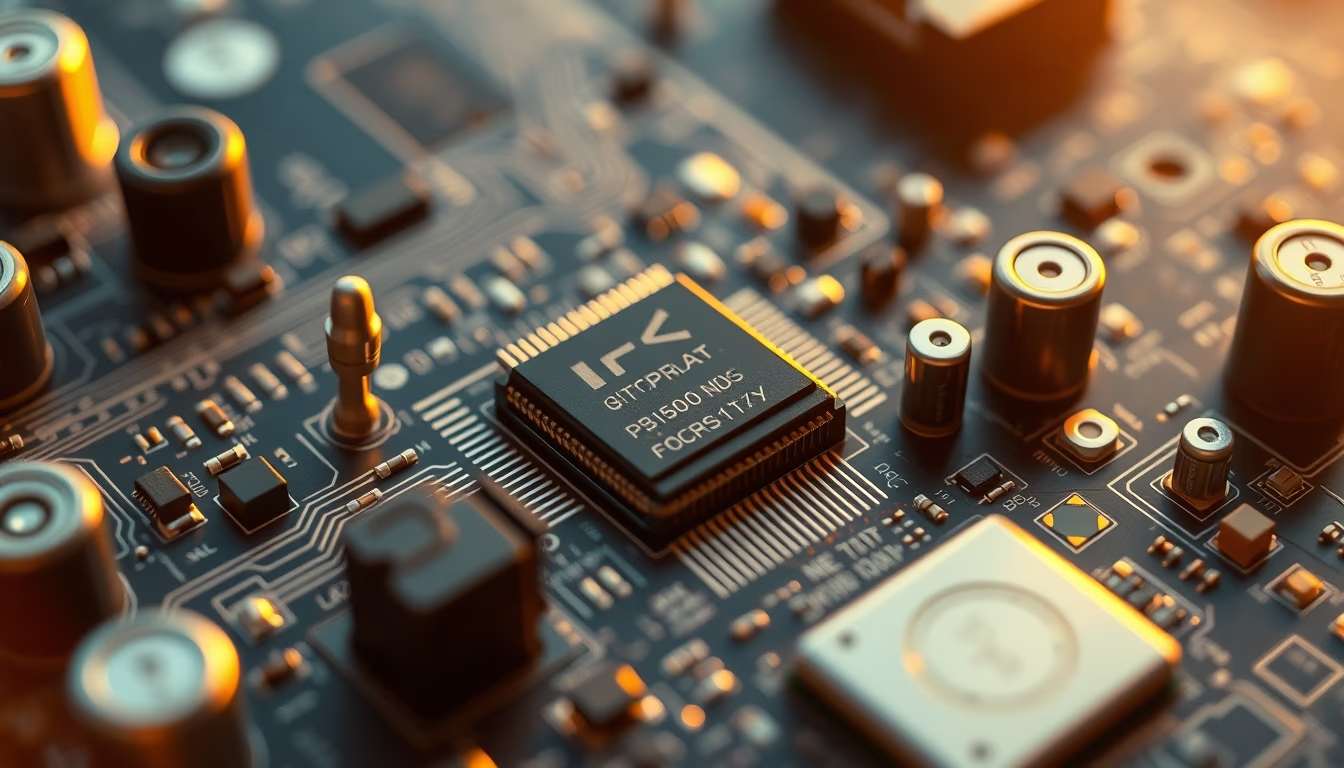
Macro photography of a printed circuit board reveals the complexity of modern microelectronics, with tiny components and conductive traces.
About this subject
Printed circuit boards (PCBs) are the foundation of virtually all modern electronic devices, from smartphones to satellites. Macro photography of circuits reveals details invisible to the naked eye: copper traces just micrometers wide, SMD (surface-mount device) components like resistors and capacitors, and precise solder joints made by robots. PCB manufacturing technology has evolved since the 1940s, when they were invented to replace manual wiring. Today, multilayer boards can have up to 60 stacked layers, interconnected by microscopic vias.
A typical PCB consists of a fiberglass substrate (FR-4), chemically etched copper layers, and a green or blue solder mask coating. Components are mounted by pick-and-place machines that position thousands of parts per hour with sub-micrometer precision. Soldering is done in reflow ovens, where solder paste melts at controlled temperatures. Macro photography can show details like solder texture, laser-etched serial numbers on chips, and even microscopic imperfections that can cause failures.
Interestingly, the green color of most PCBs is not functional but a historical choice: the green solder mask was standardized in the 1950s by IBM because it was easy to inspect and contrasted well with copper traces. Today, black, blue, red, and even transparent PCBs exist for niches like LEDs and wearables. Circuit macro photography is also used in reverse engineering, quality control, and education, helping students understand the architecture of electronic devices.
Frequently Asked Questions
What is a printed circuit board (PCB)?
A PCB is a board that connects electronic components using conductive traces etched on an insulating substrate. It replaces manual wiring, enabling compact and reliable circuits.
Why are most circuit boards green?
The green solder mask was standardized by IBM in the 1950s because it offered good contrast for visual inspection. Today, other colors are used for aesthetic or functional purposes.
How does macro photography help in circuit analysis?
It allows inspection of solder joints, identification of tiny components, and detection of defects invisible to the naked eye, useful in quality control, reverse engineering, and education.
Direct URL
https://pub-c7d6a6ea828543ac903a74a341ccb2e1.r2.dev/imagens/circuit-board-macro-photography-cinematic-wide-shot-v2.avifHow to credit
Include a visible link back to UtilizAí. Copy one of the snippets below:
<a href="https://xn--utiliza-eza.com/en/midia/imagens/circuit-board-macro-photography-cinematic-wide-shot-v2">Circuit board macro photography</a> by <a href="https://xn--utiliza-eza.com">UtilizAí</a>, licensed under <a href="https://creativecommons.org/licenses/by/4.0/">CC BY 4.0</a>.
[Circuit board macro photography](https://xn--utiliza-eza.com/en/midia/imagens/circuit-board-macro-photography-cinematic-wide-shot-v2) by [UtilizAí](https://xn--utiliza-eza.com), CC BY 4.0
License: CC-BY-4.0