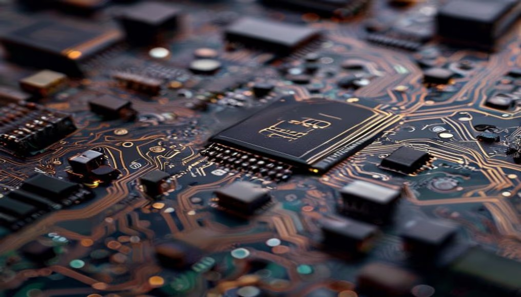
Circuit board macro photography
1344×768 · AVIF · CC BY 4.0
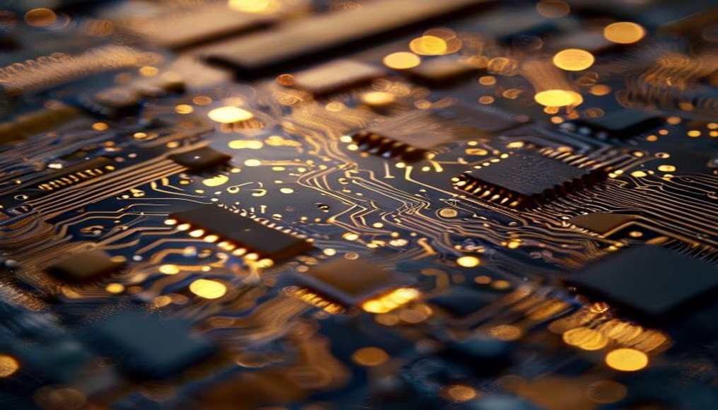
Printed circuit boards (PCBs) are essential for modern electronics. Learn how they are manufactured and their role in technology.
About this subject
Printed circuit boards, or PCBs, are the foundational platform that connects and supports electronic components in nearly all modern devices, from smartphones to medical equipment and automotive systems. Invented in 1936 by Austrian engineer Paul Eisler, PCBs revolutionized electronics by replacing manual wiring with a laminated substrate carrying conductive copper traces. Today, the global PCB production exceeds 70 billion USD annually, with China leading manufacturing, followed by Taiwan and South Korea.
The manufacturing process of a PCB starts with a base material, typically fiberglass coated with copper. Through photochemical processes, circuit traces are etched into the copper, creating conductive paths that link components. Depending on complexity, boards can have multiple layers, stacked and pressed together to allow denser circuits. Precision is critical: traces can be micrometers thick, requiring controlled environments and advanced machinery.
One fascinating aspect of PCBs is their design versatility. There are rigid, flexible, and rigid-flex boards adapted to different applications. Rigid PCBs are common in computers and TVs, while flexible ones are used in digital cameras and wearables where space is tight. Surface-mount technology (SMT) allows smaller components to be soldered directly onto the board, further enabling miniaturization. Without PCBs, modern electronics as we know it would be impossible.
Notably, PCBs also have a significant environmental impact. Improper disposal releases heavy metals like lead and tin. Directives such as the European Union's RoHS (Restriction of Hazardous Substances) regulate hazardous substances in manufacturing. PCB recycling initiatives are growing, allowing recovery of precious metals like gold and silver from discarded boards. This lifecycle is an active research area in materials engineering.
Frequently Asked Questions
What is a printed circuit board (PCB)?
A PCB is a board made of insulating material with conductive copper traces that connect electronic components. It provides mechanical support and electrical interconnection for devices like phones and computers.
How are PCBs manufactured?
Manufacturing starts with a copper-clad substrate. Photochemical processes etch the circuit traces. Multilayer boards are pressed together. Component assembly is done by soldering, often using automated machines.
What are the types of PCBs?
There are rigid, flexible, and rigid-flex PCBs. Rigid ones are most common, flexible ones allow bending for tight spaces, and rigid-flex combine both technologies in one board.
Direct URL
https://pub-c7d6a6ea828543ac903a74a341ccb2e1.r2.dev/imagens/circuit-board-macro-photography-travel-photography-v10.avifHow to credit
Include a visible link back to UtilizAí. Copy one of the snippets below:
<a href="https://xn--utiliza-eza.com/en/midia/imagens/circuit-board-macro-photography-travel-photography-v10">Circuit board macro photography</a> by <a href="https://xn--utiliza-eza.com">UtilizAí</a>, licensed under <a href="https://creativecommons.org/licenses/by/4.0/">CC BY 4.0</a>.
[Circuit board macro photography](https://xn--utiliza-eza.com/en/midia/imagens/circuit-board-macro-photography-travel-photography-v10) by [UtilizAí](https://xn--utiliza-eza.com), CC BY 4.0
License: CC-BY-4.0