Wafer silicon photolithography
1344×768 · AVIF · CC BY 4.0
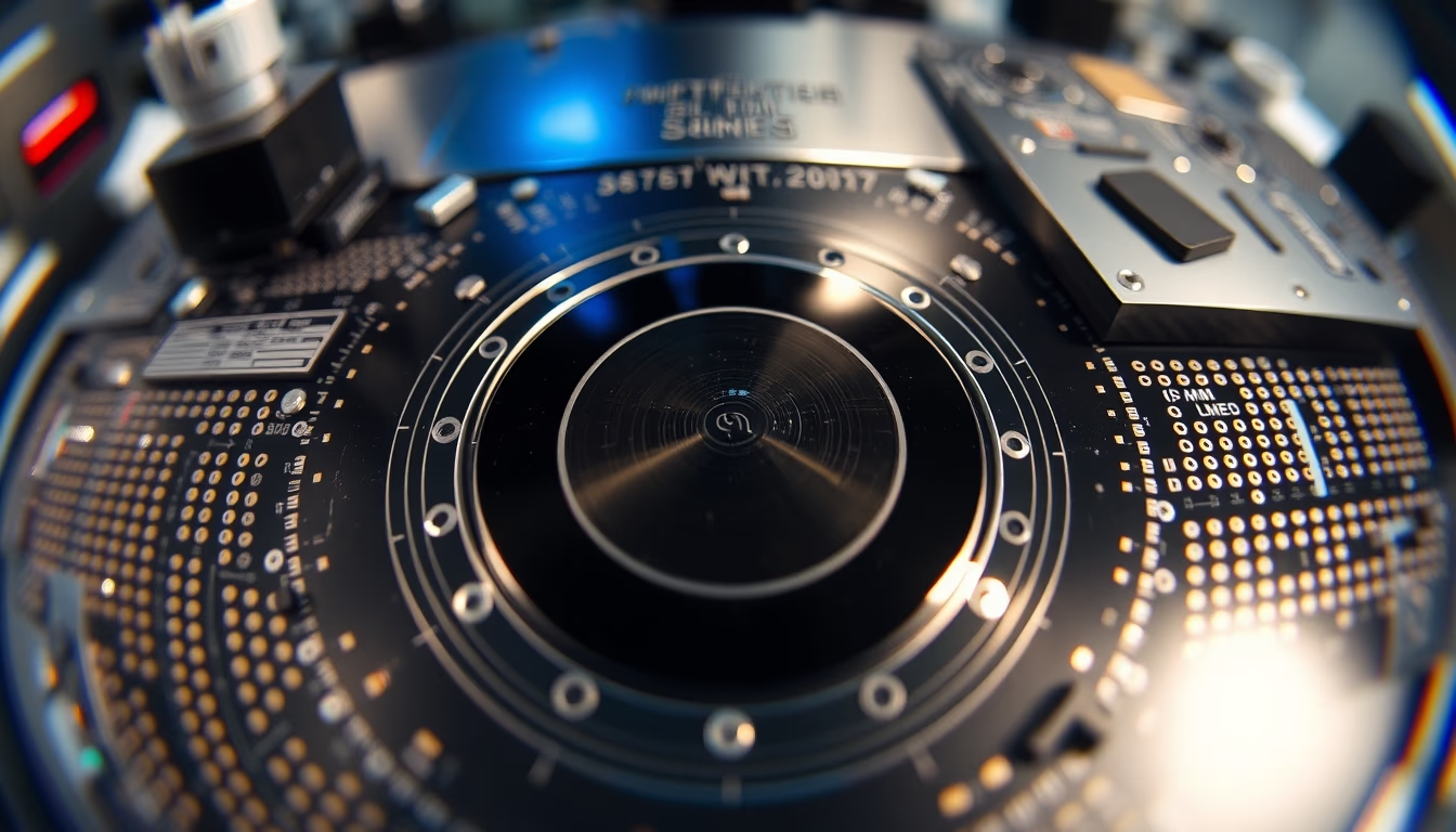
Silicon wafer photolithography is the core process in integrated circuit fabrication, using ultraviolet light to transfer nanoscale patterns, enabling modern chips.
About this subject
Photolithography is the core process in semiconductor manufacturing, where intricate circuit patterns are transferred onto a silicon wafer. The wafer is first coated with a photoresist, a light-sensitive material that changes property when exposed. Then, the wafer is aligned under a photomask containing the circuit design, and ultraviolet (UV) light is projected through the mask, selectively exposing the photoresist. Exposed areas become either soluble or insoluble (depending on the resist type), enabling the pattern to be revealed after chemical development. This pattern is then transferred to the silicon via etching or thin-film deposition, building chip layers.
This process is repeated dozens of times, aligning with sub-nanometer precision, to construct three-dimensional transistor and interconnect structures. Photolithography was pivotal to Moore's Law, allowing continuous transistor size reduction. In the 1980s, 1990s, UV light from mercury lamps (i-line, 365 nm) was used; today, extreme ultraviolet lithography (EUV) uses 13.5 nm wavelengths, generated from tin plasma sources, to etch features as small as 5 nm.
A fascinating detail: the photoacoustics of UV exposure demand strict temperature control, as a 0.1 °C variation can distort the wafer enough to cause misalignment. Moreover, photomasks are made of quartz and chromium, each costing millions of dollars because they must be defect-free. Without photolithography, modern processors, memories, and sensors would not exist, it is the cornerstone of nanotechnology powering the digital age.
Frequently Asked Questions
What is photolithography in chip manufacturing?
It is a process that uses ultraviolet light to transfer circuit patterns from a photomask onto a silicon wafer coated with photoresist, building transistor and interconnect layers.
Why is photolithography important for semiconductors?
It enables the creation of nanoscale structures with high precision, allowing continuous transistor miniaturization and performance gains, as predicted by Moore's Law.
What are the main steps of photolithography?
The steps include wafer cleaning, photoresist coating, alignment and exposure to UV light through a mask, chemical development, etching or deposition, and resist stripping, repeated for each chip layer.
Direct URL
https://pub-c7d6a6ea828543ac903a74a341ccb2e1.r2.dev/imagens/wafer-silicon-photolithography-fish-eye-wide-angle-p8.avifHow to credit
Include a visible link back to UtilizAí. Copy one of the snippets below:
<a href="https://xn--utiliza-eza.com/en/midia/imagens/wafer-silicon-photolithography-fish-eye-wide-angle-p8">Wafer silicon photolithography</a> by <a href="https://xn--utiliza-eza.com">UtilizAí</a>, licensed under <a href="https://creativecommons.org/licenses/by/4.0/">CC BY 4.0</a>.
[Wafer silicon photolithography](https://xn--utiliza-eza.com/en/midia/imagens/wafer-silicon-photolithography-fish-eye-wide-angle-p8) by [UtilizAí](https://xn--utiliza-eza.com), CC BY 4.0
License: CC-BY-4.0





