Wafer silicon photolithography
1344×768 · AVIF · CC BY 4.0
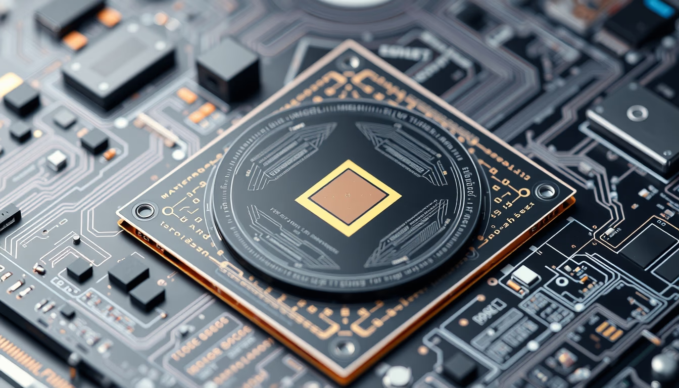
Understand the photolithography process on silicon wafers, a crucial step in manufacturing chips and integrated circuits.
About this subject
Photolithography is a fundamental process in integrated circuit fabrication, responsible for transferring microscopic patterns onto the surface of a silicon wafer. Using ultraviolet light, a mask containing the circuit design is projected onto the wafer, which has been previously coated with a photosensitive material called photoresist. The exposed areas undergo a chemical reaction, becoming either soluble or insoluble in a developer, depending on the type of resist (positive or negative). After development, the wafer undergoes etching processes to remove unprotected areas, creating the conductive and insulating structures that form transistors and interconnects.
This process is repeated dozens of times on each wafer, with different masks and layers, to build complex three-dimensional circuits. The precision of photolithography is measured in nanometers, the shorter the wavelength of light used, the finer the lines that can be etched. Modern technologies employ extreme ultraviolet (EUV) light with wavelengths of 13.5 nm, enabling the production of chips with transistors as small as 5 nm or less.
The evolution of photolithography is directly linked to Moore’s Law, which predicts the doubling of transistor count every two years. From the 1960s when the first integrated circuits were fabricated using manual processes, to today, automation and improvements in lenses, light sources, and photoresist materials have enabled mass production of increasingly powerful and cost-effective chips. Companies like ASML, Nikon, and Canon dominate the lithography equipment market, with billions invested in research and development.
Beyond the semiconductor industry, photolithography is used in microelectronics, MEMS (Micro-Electro-Mechanical Systems) fabrication, sensors, and optical devices. Strict wafer cleanliness and particle control are essential to avoid defects, as a single dust particle can ruin an entire chip. The cleanrooms where lithography occurs maintain extremely low contamination levels, typically ISO class 1 or 2.
Frequently Asked Questions
What is photolithography?
It is a process used in integrated circuit fabrication to transfer geometric patterns from a mask onto the surface of a silicon wafer, using light and a photosensitive material called photoresist.
Why is photolithography so important in chip manufacturing?
It enables the creation of microscopic structures with nanometric precision, essential for miniaturizing transistors and increasing component density, following Moore's Law.
What are the main steps of photolithography?
The steps include: wafer cleaning, photoresist coating, exposure to light through a mask, development to remove exposed or unexposed areas, and etching to transfer the pattern to the substrate.
Direct URL
https://pub-c7d6a6ea828543ac903a74a341ccb2e1.r2.dev/imagens/wafer-silicon-photolithography-isometric-flat-lay-p7.avifHow to credit
Include a visible link back to UtilizAí. Copy one of the snippets below:
<a href="https://xn--utiliza-eza.com/en/midia/imagens/wafer-silicon-photolithography-isometric-flat-lay-p7">Wafer silicon photolithography</a> by <a href="https://xn--utiliza-eza.com">UtilizAí</a>, licensed under <a href="https://creativecommons.org/licenses/by/4.0/">CC BY 4.0</a>.
[Wafer silicon photolithography](https://xn--utiliza-eza.com/en/midia/imagens/wafer-silicon-photolithography-isometric-flat-lay-p7) by [UtilizAí](https://xn--utiliza-eza.com), CC BY 4.0
License: CC-BY-4.0





