Circuit traces pcb closeup
1344×768 · AVIF · CC BY 4.0
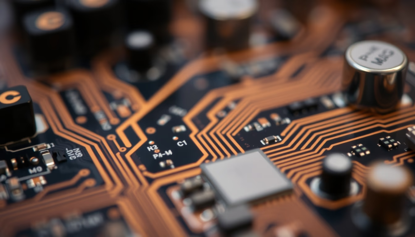
Close-up of printed circuit board traces reveals the precision of PCB manufacturing, essential for modern electronic devices.
About this subject
Circuit traces are the thin copper layers that connect electronic components on a printed circuit board (PCB). They are created through chemical or mechanical processes such as etching or milling, and their width and spacing follow strict specifications to avoid shorts and ensure signal integrity. PCBs are the foundation of virtually all electronic devices, from smartphones to medical and aerospace equipment.
PCB manufacturing involves several steps: design in CAD software, lamination of copper onto a fiberglass substrate (FR4), application of photoresist, exposure to UV light to transfer the circuit pattern, development, and etching of exposed copper. The resulting traces typically have thicknesses ranging from 35 to 105 micrometers. In high-density boards, traces become extremely thin, sometimes less than 100 micrometers wide, requiring precise alignment during exposure.
The tilt-shift miniature effect applied to the image simulates a shallow depth of field, making the board look like a miniature model. This highlights the complexity and minute detailing of the traces, emphasizing the engineering behind circuits. The tilt-shift technique is achieved with special lenses or digital post-processing, and here it serves to underscore the intricacies of circuit design.
Historically, the first PCBs emerged in the 1940s to replace hand wiring, and today the global PCB market exceeds $70 billion annually. The evolution of circuit traces has followed Moore's Law, with multilayer boards and microscopic interconnects enabling increasingly powerful and compact devices. Trace quality is critical for electrical performance, heat dissipation, and long-term reliability.
Frequently Asked Questions
What are printed circuit board traces?
They are thin copper layers etched onto a PCB that connect electronic components, enabling signal and power transmission.
How are PCB traces manufactured?
The process involves CAD design, copper lamination on substrate, photoresist application, UV exposure, development, and chemical etching. Modern boards use multiple layers and advanced lithography.
Why are trace width and spacing important?
Too thin traces can overheat or cause excessive resistance; inadequate spacing may cause shorts. Precise parameters ensure signal integrity and reliability at high frequencies.
Direct URL
https://pub-c7d6a6ea828543ac903a74a341ccb2e1.r2.dev/imagens/circuit-traces-pcb-closeup-tilt-shift-miniature-p8.avifHow to credit
Include a visible link back to UtilizAí. Copy one of the snippets below:
<a href="https://xn--utiliza-eza.com/en/midia/imagens/circuit-traces-pcb-closeup-tilt-shift-miniature-p8">Circuit traces pcb closeup</a> by <a href="https://xn--utiliza-eza.com">UtilizAí</a>, licensed under <a href="https://creativecommons.org/licenses/by/4.0/">CC BY 4.0</a>.
[Circuit traces pcb closeup](https://xn--utiliza-eza.com/en/midia/imagens/circuit-traces-pcb-closeup-tilt-shift-miniature-p8) by [UtilizAí](https://xn--utiliza-eza.com), CC BY 4.0
License: CC-BY-4.0





