Circuit traces pcb closeup
1344×768 · AVIF · CC BY 4.0
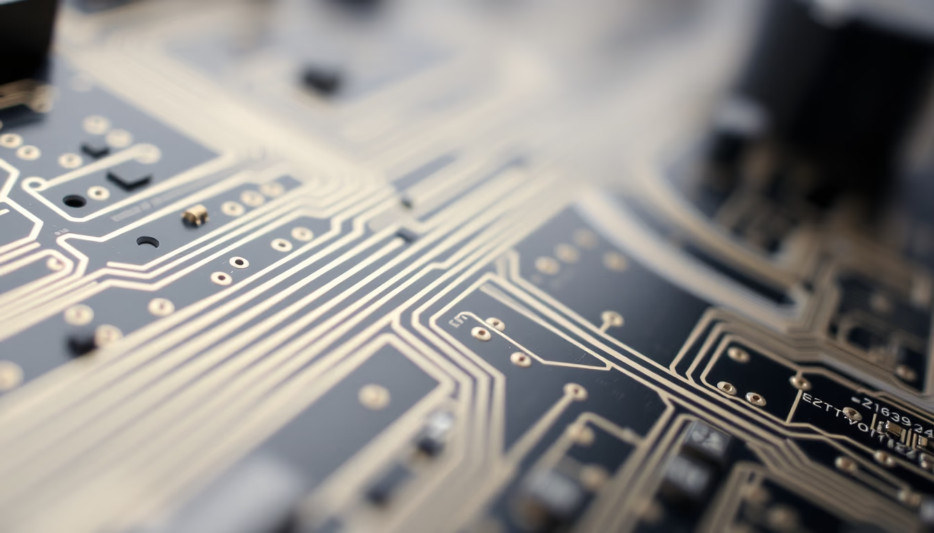
Circuit traces on a printed circuit board (PCB) are thin copper pathways connecting electronic components, forming the electrical backbone of modern devices.
About this subject
Circuit traces, also known as PCB traces, are conductive copper pathways etched onto an insulating substrate, typically fiberglass epoxy (FR-4). They replace traditional wires, allowing precise and compact connections in electronic devices. The manufacturing process starts with a copper-clad laminate covered with photoresist. Ultraviolet light exposure through a photomask defines the trace pattern, and chemical etching removes unprotected copper, leaving only the desired traces. Standard copper thickness is measured in ounces per square foot (oz/ft²): 1 oz equals approximately 35 µm (1.4 mils). For high-current designs, thicker traces like 2 oz or more are used.
Traces can be single-layer (single-sided PCBs) or multilayer, where multiple copper layers are interleaved with insulators and connected by plated through-holes (vias). Modern PCBs with over 50 layers are common in servers and telecom equipment. Trace width and spacing follow design rules to avoid shorts, maintain controlled impedance, and minimize electromagnetic interference. For high-frequency signals, such as RF circuits, traces are designed as microstrip or stripline with dimensions calculated for characteristic impedance (e.g., 50 Ω).
Historically, the development of the PCB revolutionized electronics from the 1940s, with Paul Eisler's invention of the etching process. Today, trace fabrication achieves micrometer tolerances using photolithography and electrodeposition. Trace surfaces may receive finishes like OSP (Organic Solderability Preservative), HASL (Hot Air Solder Leveling), or gold plating to protect copper and enhance solderability. High-performance boards use high-purity electrolytic copper (99.9%) to minimize electrical resistance and signal loss.
Beyond conductivity, traces must withstand thermal and mechanical stress during soldering and operation. Substrate thermal expansion can cause trace cracks if not carefully designed, hence automotive and aerospace applications use materials like polyimide. Trace inspection involves electrical testing (continuity and isolation) and X-ray inspection for multilayer boards. Ongoing miniaturization demands ever-finer traces (below 50 µm) and new methods such as 3D printing of conductive circuits.
Frequently Asked Questions
What is the typical thickness of a copper trace on a PCB?
Thickness is measured in ounces per square foot (oz/ft²). The most common is 1 oz (approximately 35 µm or 1.4 mils). For higher currents, 2 oz (70 µm) or thicker is used.
How are PCB traces manufactured?
The primary process is photolithography combined with chemical etching. A copper-clad board is coated with photoresist, exposed to UV light through a photomask, and then chemically etched to remove unprotected copper, leaving only the desired traces.
Why do some PCBs have multiple layers of traces?
Multiple layers allow higher component density and complex connections in a small space, improve signal integrity (with dedicated ground and power planes), and reduce interference. Server PCBs can have over 50 layers.
Direct URL
https://pub-c7d6a6ea828543ac903a74a341ccb2e1.r2.dev/imagens/circuit-traces-pcb-closeup-studio-still-life-p4.avifHow to credit
Include a visible link back to UtilizAí. Copy one of the snippets below:
<a href="https://xn--utiliza-eza.com/en/midia/imagens/circuit-traces-pcb-closeup-studio-still-life-p4">Circuit traces pcb closeup</a> by <a href="https://xn--utiliza-eza.com">UtilizAí</a>, licensed under <a href="https://creativecommons.org/licenses/by/4.0/">CC BY 4.0</a>.
[Circuit traces pcb closeup](https://xn--utiliza-eza.com/en/midia/imagens/circuit-traces-pcb-closeup-studio-still-life-p4) by [UtilizAí](https://xn--utiliza-eza.com), CC BY 4.0
License: CC-BY-4.0





