Chip die exposed silicon
1344×768 · AVIF · CC BY 4.0
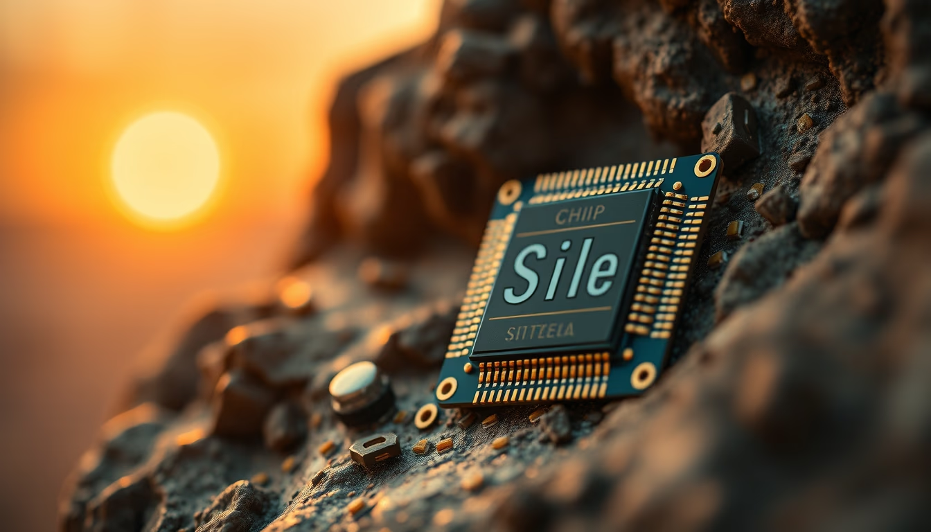
An exposed chip die reveals the silicon heart of an integrated circuit, where microscopic transistors handle billions of operations per second.
About this subject
A chip die, also known as a silicon die, is the central piece of any integrated circuit. It is a small square or rectangle of crystalline silicon, upon which millions or billions of transistors, capacitors, and resistors are fabricated through a complex lithographic process. This component is the functional unit of the chip before being encapsulated in resin or ceramic for mechanical and thermal protection.
The manufacturing of a die starts with an ultra-pure silicon ingot, sliced into thin wafers. Each wafer undergoes dozens of steps: doping, photolithography, etching, and deposition of conductive layers. At the end, the wafer is electrically tested and sawed to separate individual dies. One of the biggest challenges in the industry is minimizing defects, as a single dust particle can ruin an entire die.
Exposing the die, as seen in the image, is common in semiconductor photography or engineering reverse engineering labs. Unlike an encapsulated chip, the exposed die reveals the metalized structure (aluminum or copper traces) and the silicon substrate. The multicolored appearance, often observed in electron microscopy, results from light diffraction in the dielectric layers. Major companies like Intel, AMD, and TSMC invest billions in research to reduce transistor size and increase density, following Moore's Law.
Trivia: the largest commercial die ever manufactured belongs to an Nvidia GPU, with over 800 mm² of area, while modern CPUs have dies around 100 to 300 mm². Exposing the die is crucial for failure analysis and design validation, as it allows direct optical inspection of internal layers.
Frequently Asked Questions
What is a chip die?
A chip die is the silicon substrate where the integrated circuit is fabricated. It contains all transistors and interconnections that perform the chip's functions, before being encapsulated for protection.
Why does the exposed die appear colorful?
The iridescent colors are caused by light diffraction in the thin oxide and metal layers deposited on the silicon, similar to the effect seen in soap bubbles.
What is the difference between a die and an encapsulated chip?
The die is the bare semiconductor component, fragile and sensitive. The encapsulated chip encases the die in resin or ceramic, adding pins for electrical connection and protection.
Direct URL
https://pub-c7d6a6ea828543ac903a74a341ccb2e1.r2.dev/imagens/chip-die-exposed-silicon-travel-photography-p0.avifHow to credit
Include a visible link back to UtilizAí. Copy one of the snippets below:
<a href="https://xn--utiliza-eza.com/en/midia/imagens/chip-die-exposed-silicon-travel-photography-p0">Chip die exposed silicon</a> by <a href="https://xn--utiliza-eza.com">UtilizAí</a>, licensed under <a href="https://creativecommons.org/licenses/by/4.0/">CC BY 4.0</a>.
[Chip die exposed silicon](https://xn--utiliza-eza.com/en/midia/imagens/chip-die-exposed-silicon-travel-photography-p0) by [UtilizAí](https://xn--utiliza-eza.com), CC BY 4.0
License: CC-BY-4.0





