Chip die exposed silicon
1344×768 · AVIF · CC BY 4.0
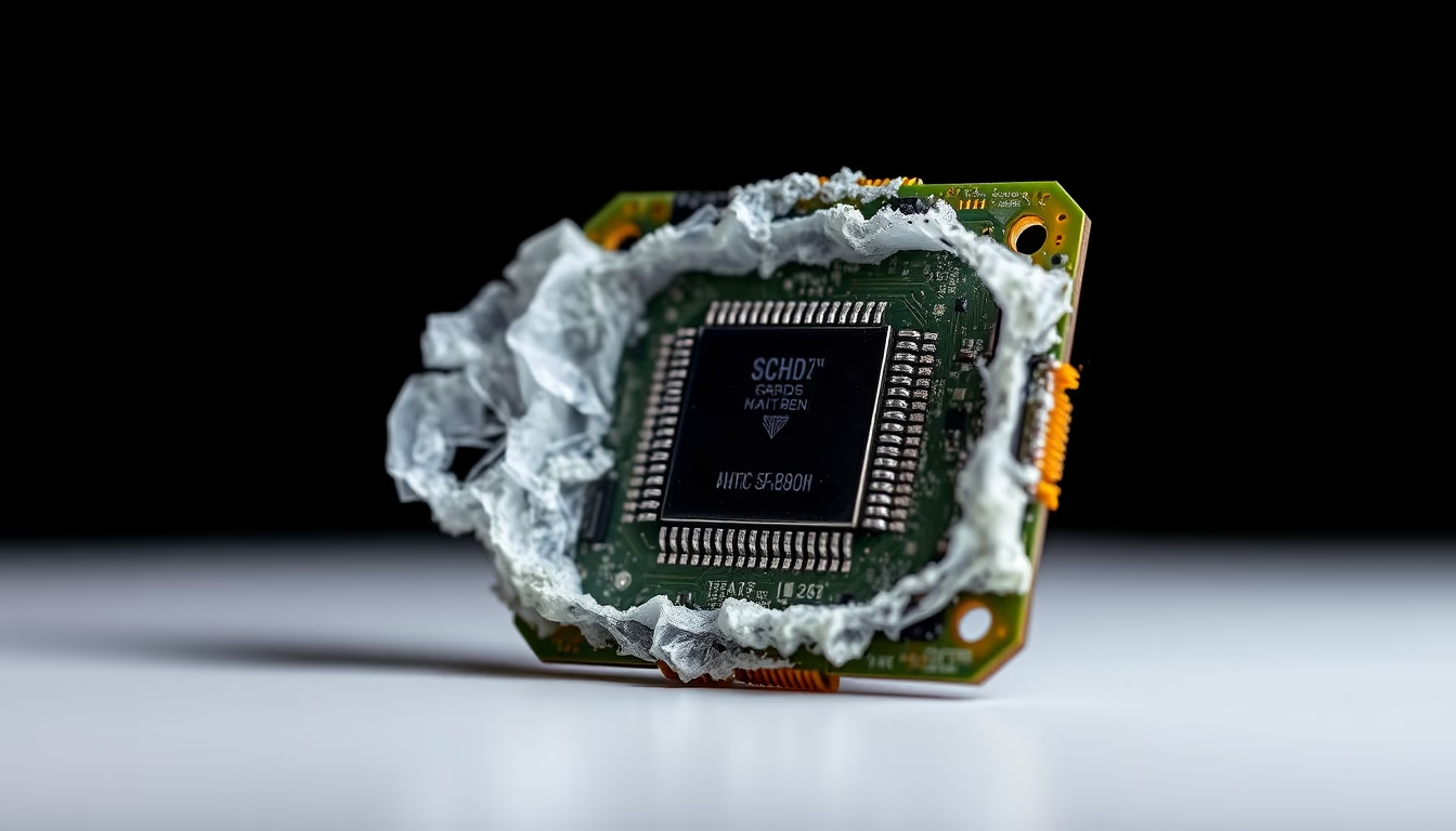
Exposed silicon chip die reveals the complexity of integrated circuits, the core of modern electronic devices.
About this subject
The chip die, also known as a silicon die, is the heart of any integrated circuit. It is a small rectangular block of monocrystalline silicon onto which billions of transistors, resistors, and other electronic components are fabricated. Exposing the die reveals the polished silicon surface, often with metallic interconnection patterns visible as thin gold or silver lines.
The manufacturing of a chip die involves complex processes like photolithography, doping, and etching. Silicon is chosen for its semiconducting properties and abundance in the Earth's crust. A single silicon wafer can contain hundreds or thousands of dies, later cut and packaged in protective enclosures. The studio still life of an exposed die serves as an educational example for engineers and enthusiasts, highlighting the miniaturization achieved by the industry.
Moore's Law, an observation by Gordon Moore in 1965, predicted that the number of transistors on a chip would double approximately every two years. This prediction guided microelectronics development for decades, resulting in modern chips with tens of billions of transistors on areas smaller than a fingernail. The exposed silicon is a testament to precision engineering, where defects in the crystal structure can render the device nonfunctional.
Interestingly, silicon is the second most abundant element on Earth, but the purity required for semiconductors is so extreme that the refining process can take weeks. The die exposure also reveals the characteristic bluish-gray color of silicon and the oxide layers that insulate structures. This image is an icon of the digital age, representing the materialization of billions of logical operations per second.
Frequently Asked Questions
Why is silicon the most used material in chips?
Silicon is an abundant, low-cost semiconductor with stable electrical properties. It also forms a natural oxide (SiO2) that serves as an excellent insulator, essential for manufacturing MOS transistors.
What does 'exposed chip die' mean?
The die is the silicon piece containing the integrated circuit. 'Exposed' means it is not packaged, allowing direct view of the silicon surface and metal interconnections, common in technical analysis or studio photography.
How many transistors fit in a modern chip die?
Modern chips can contain tens of billions of transistors. For instance, the Apple M1 Ultra has approximately 114 billion transistors in a single package.
Direct URL
https://pub-c7d6a6ea828543ac903a74a341ccb2e1.r2.dev/imagens/chip-die-exposed-silicon-studio-still-life-p6.avifHow to credit
Include a visible link back to UtilizAí. Copy one of the snippets below:
<a href="https://xn--utiliza-eza.com/en/midia/imagens/chip-die-exposed-silicon-studio-still-life-p6">Chip die exposed silicon</a> by <a href="https://xn--utiliza-eza.com">UtilizAí</a>, licensed under <a href="https://creativecommons.org/licenses/by/4.0/">CC BY 4.0</a>.
[Chip die exposed silicon](https://xn--utiliza-eza.com/en/midia/imagens/chip-die-exposed-silicon-studio-still-life-p6) by [UtilizAí](https://xn--utiliza-eza.com), CC BY 4.0
License: CC-BY-4.0





