Chip die exposed silicon
1344×768 · AVIF · CC BY 4.0
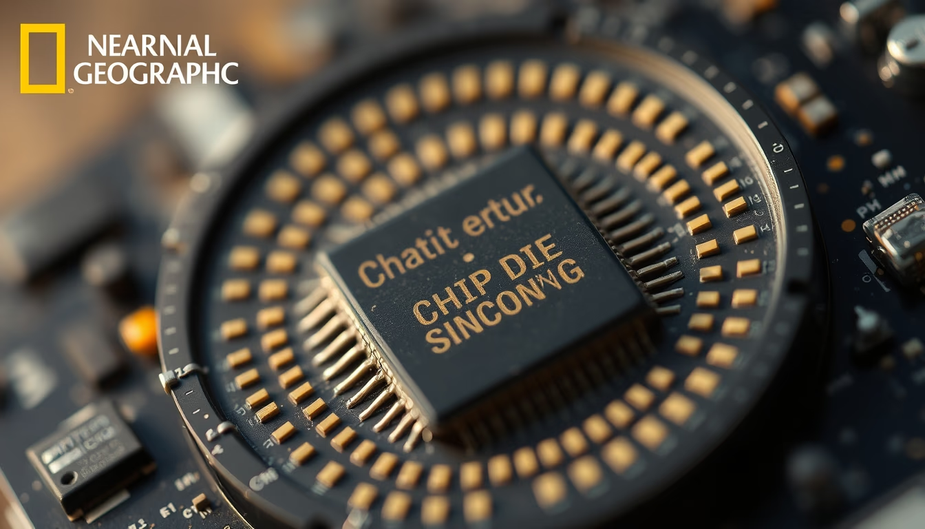
The exposed chip die is the silicon heart of an integrated circuit, revealing the complex architecture of transistors at a microscopic scale.
About this subject
The chip die, also known as the silicon matrix, is the core of any integrated circuit. It is a small rectangular or square piece of monocrystalline silicon where billions of transistors and interconnections are lithographed in stacked layers. At the heart of every microprocessor, memory chip, or sensor, the die performs all logical and storage operations.
Its manufacturing, called wafer fabrication, begins with extracting high-purity silicon from quartz sand. The silicon is melted and crystallized into cylindrical ingots, which are sliced into ultra-thin wafers. On each wafer, dozens or hundreds of dies are created through photolithography, material deposition, and controlled doping. After production, each die is electrically tested and then separated from the wafer by diamond blade sawing.
The chip die's importance to modern technology is immeasurable. From smartphones to satellites, all digital devices depend on silicon dies. Moore's Law, the historical observation that the number of transistors on a chip doubles approximately every two years, drove progress for decades, though physical challenges are now slowing it. Today, advanced dies use fabrication nodes of 7 nm or 5 nm, achieving transistor densities over 100 million per square millimeter.
Interestingly, exposing the naked die (without packaging) is common in reverse engineering and macro photography. The geometric pattern on the surface results from multiple metal and dielectric layers forming interconnections between transistors. The iridescent colors seen in some images are due to thin oxide layers causing light interference, a phenomenon used in labs to measure thin film thicknesses.
Frequently Asked Questions
What is a chip die?
It is the silicon matrix containing the actual integrated circuit, with billions of miniaturized transistors. It is usually encapsulated in plastic or ceramic for protection.
How is a chip die manufactured?
The process starts with silicon purification, ingot growth, wafer slicing, photolithography, doping, and layer deposition. After fabrication, dies are tested and separated from the wafer.
Why do chip dies show iridescent colors?
The colors result from light interference in thin silicon oxide layers on the surface. Each thickness produces a specific color, useful for quality control.
Direct URL
https://pub-c7d6a6ea828543ac903a74a341ccb2e1.r2.dev/imagens/chip-die-exposed-silicon-national-geographic-style-p1.avifHow to credit
Include a visible link back to UtilizAí. Copy one of the snippets below:
<a href="https://xn--utiliza-eza.com/en/midia/imagens/chip-die-exposed-silicon-national-geographic-style-p1">Chip die exposed silicon</a> by <a href="https://xn--utiliza-eza.com">UtilizAí</a>, licensed under <a href="https://creativecommons.org/licenses/by/4.0/">CC BY 4.0</a>.
[Chip die exposed silicon](https://xn--utiliza-eza.com/en/midia/imagens/chip-die-exposed-silicon-national-geographic-style-p1) by [UtilizAí](https://xn--utiliza-eza.com), CC BY 4.0
License: CC-BY-4.0





