Chip die exposed silicon
1344×768 · AVIF · CC BY 4.0
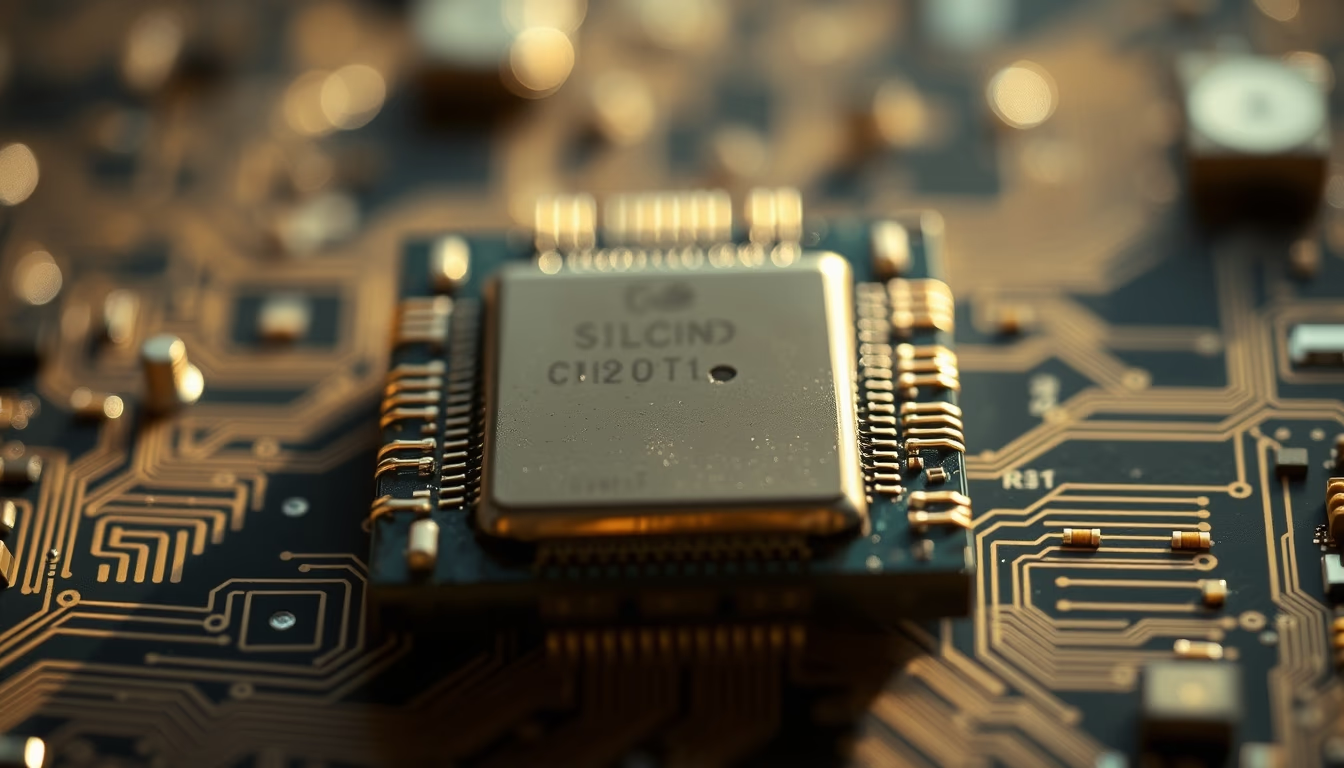
The chip die is the silicon wafer piece that contains the integrated circuit, the heart of any modern processor.
About this subject
The chip die, also called a silicon die, is the fundamental unit of any integrated circuit. It is obtained from a monocrystalline silicon wafer through a complex process of photolithography, doping, and layer deposition to form transistors, resistors, and metal interconnects. Each die can contain billions of transistors, as in modern processors, and is individually tested before being encapsulated in plastic or ceramic packaging.
Exposing the die reveals its shiny, colorful structure, resulting from dielectric and metal layers. This appearance is often exploited in documentary photography to showcase the ingenuity of microelectronics. Silicon is the most used material due to its abundance and semiconducting properties, but substrates like gallium arsenide are used for high-speed applications.
Die fabrication requires cleanrooms of class 10 or better, where particle count is rigorously controlled. Each die's cost depends on wafer size and process yield. For example, a 300 mm wafer can yield hundreds of dies, but defects can significantly reduce production. Continuous miniaturization, following Moore's Law, has led to dies with 3 nm or smaller nodes.
Interestingly, photography of exposed dies is used by engineers for failure analysis and by enthusiasts to appreciate engineering art. High-resolution images of dies, such as those captured by electron microscopes, reveal details resembling city maps, with interconnect streets and functional blocks.
Frequently Asked Questions
What is a chip die?
It is the silicon piece containing the integrated circuit of a chip, before encapsulation.
Why does a chip die show different colors?
Colors come from thin dielectric and metal layers; they interfere with light, creating characteristic iridescent hues.
Why is photographing exposed dies important?
It helps in defect and failure analysis, and also documents the complexity and beauty of microelectronics.
Direct URL
https://pub-c7d6a6ea828543ac903a74a341ccb2e1.r2.dev/imagens/chip-die-exposed-silicon-documentary-photography-p11.avifHow to credit
Include a visible link back to UtilizAí. Copy one of the snippets below:
<a href="https://xn--utiliza-eza.com/en/midia/imagens/chip-die-exposed-silicon-documentary-photography-p11">Chip die exposed silicon</a> by <a href="https://xn--utiliza-eza.com">UtilizAí</a>, licensed under <a href="https://creativecommons.org/licenses/by/4.0/">CC BY 4.0</a>.
[Chip die exposed silicon](https://xn--utiliza-eza.com/en/midia/imagens/chip-die-exposed-silicon-documentary-photography-p11) by [UtilizAí](https://xn--utiliza-eza.com), CC BY 4.0
License: CC-BY-4.0





