Chip die exposed silicon
1344×768 · AVIF · CC BY 4.0
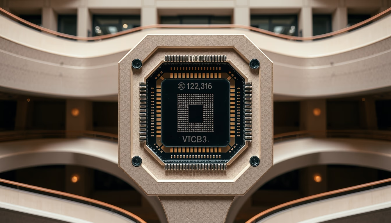
Micrograph of an exposed silicon chip die, revealing the complex architecture of integrated circuits at nanometer scale.
About this subject
The exposed silicon chip die is the heart of any modern electronic device, from smartphones to supercomputers. It consists of a small rectangle of silicon, typically a few square millimeters, onto which billions of transistors are etched. Manufacturing involves processes such as photolithography, doping, and layer deposition, carried out in clean rooms with atomic precision. Companies like TSMC and Intel dominate this technology, with fabrication nodes reaching 3 nanometers.
The architecture visible in a photograph of an exposed chip die reveals repetitive geometric patterns, which represent functional blocks: processing units, cache memory, memory controllers, and interconnects. Each color or texture may indicate different materials or metallization layers. These patterns are designed by engineers using CAD (Computer-Aided Design) tools and verified through complex simulations.
The term “die” originates from the wafer dicing process: a silicon wafer is cut into dozens or hundreds of individual dies. Each die is then encapsulated into a package for protection and electrical connections. Photography of exposed dies is common in failure analysis and reverse engineering, but has also gained appreciation as architectural art due to its symmetric and detailed aesthetics.
Continuous miniaturization, described by Moore's Law, doubled the number of transistors every two years. However, since 2010, physical challenges such as leakage currents and heat dissipation have slowed this progression. Innovations like extreme ultraviolet (EUV) lithography and 3D die stacking are now essential to maintain technological advancement.
Frequently Asked Questions
What is an exposed silicon chip die?
It is the bare silicon piece, without packaging, that contains the integrated circuit. It is the active part of the chip where transistors and interconnects are fabricated.
How is a chip die photograph taken?
Typically, a scanning electron microscope (SEM) or a high-resolution camera attached to an optical microscope is used. The die is illuminated with grazing light to highlight the topography and patterns.
Why are chips called 'dies'?
The name originates from the wafer dicing process: the silicon wafer is cut into squares or rectangles called 'dies'. Each die becomes an individual chip after packaging.
Direct URL
https://pub-c7d6a6ea828543ac903a74a341ccb2e1.r2.dev/imagens/chip-die-exposed-silicon-architectural-photography-p3.avifHow to credit
Include a visible link back to UtilizAí. Copy one of the snippets below:
<a href="https://xn--utiliza-eza.com/en/midia/imagens/chip-die-exposed-silicon-architectural-photography-p3">Chip die exposed silicon</a> by <a href="https://xn--utiliza-eza.com">UtilizAí</a>, licensed under <a href="https://creativecommons.org/licenses/by/4.0/">CC BY 4.0</a>.
[Chip die exposed silicon](https://xn--utiliza-eza.com/en/midia/imagens/chip-die-exposed-silicon-architectural-photography-p3) by [UtilizAí](https://xn--utiliza-eza.com), CC BY 4.0
License: CC-BY-4.0





