Wafer silicon photolithography
1344×768 · AVIF · CC BY 4.0
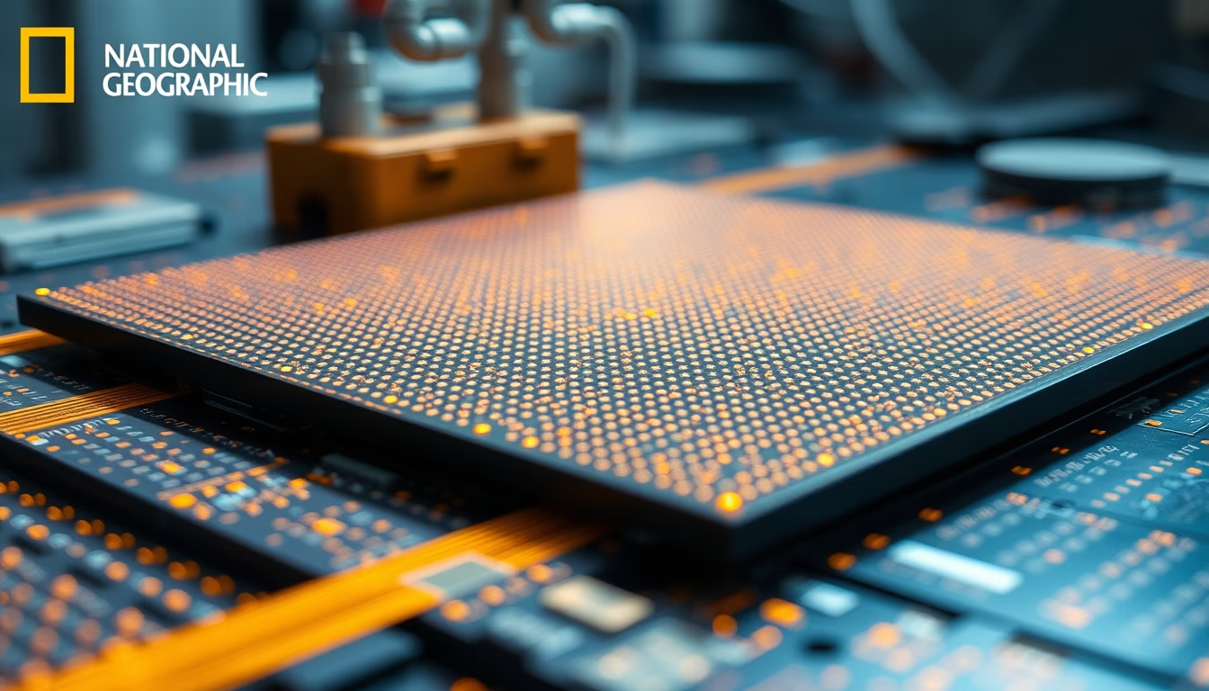
Silicon wafer photolithography is the fundamental process that etches microscopic circuits onto silicon wafers, the basis of modern chip manufacturing.
About this subject
Silicon wafer photolithography is the central technology in integrated circuit manufacturing, responsible for transferring nanometer-scale patterns from a photomask to a silicon wafer coated with a photosensitive material called photoresist. The process begins with wafer cleaning, followed by spin-coating a uniform layer of liquid photoresist. Then, the wafer is exposed to ultraviolet light through a mask containing the circuit design. The light alters the photoresist's solubility, allowing exposed areas to be removed during development, revealing the desired pattern.
The importance of photolithography lies in its continuous miniaturization capability, which drove Moore's Law. Since the technique's invention in the 1950s, inspired by optical lithography used in printing, the light wavelengths used have dramatically decreased: from mercury lamps (436 nm) to deep ultraviolet (193 nm) and, more recently, to extreme ultraviolet (EUV) at 13.5 nm. This reduction enables transistors with dimensions below 10 nm, found in modern processors.
A technical curiosity is the need for precise alignment between successive chip layers. Each photolithography step requires that the current pattern overlays previous ones with nanometer accuracy, using alignment systems based on reference marks etched into the wafer. Additionally, the choice of photoresist, positive or negative, determines whether the exposed area is removed or hardened, influencing the subsequent etching step that removes unprotected material.
The process is repeated dozens of times to build the multiple layers of a modern chip, such as those used in smartphones and computers. Photolithography also finds applications in other semiconductor devices, like image sensors and solar cells. With the move to EUV, challenges increase: lenses must be made of multilayer mirrors, and the entire process occurs in a vacuum to prevent light absorption by air.
Frequently Asked Questions
What is photolithography?
Photolithography is a process that uses light to transfer a geometric pattern from a photomask to a surface coated with photoresist, typically a silicon wafer. It is the fundamental technique for defining integrated circuits in semiconductor manufacturing.
Why is photoresist important in photolithography?
Photoresist is a photosensitive material that undergoes a chemical reaction when exposed to light, becoming soluble or insoluble in specific solvents. This change allows only the desired areas to be preserved or removed, forming the circuit pattern.
How does EUV (extreme ultraviolet) lithography differ from traditional UV lithography?
EUV lithography uses light with a wavelength of 13.5 nm, much shorter than the 193 nm of deep UV lithography. This enables ultra-high resolution patterning, essential for technology nodes below 7 nm. However, it requires vacuum systems and special reflective mirrors because EUV light is absorbed by air.
Direct URL
https://pub-c7d6a6ea828543ac903a74a341ccb2e1.r2.dev/imagens/wafer-silicon-photolithography-national-geographic-style-p0.avifHow to credit
Include a visible link back to UtilizAí. Copy one of the snippets below:
<a href="https://xn--utiliza-eza.com/en/midia/imagens/wafer-silicon-photolithography-national-geographic-style-p0">Wafer silicon photolithography</a> by <a href="https://xn--utiliza-eza.com">UtilizAí</a>, licensed under <a href="https://creativecommons.org/licenses/by/4.0/">CC BY 4.0</a>.
[Wafer silicon photolithography](https://xn--utiliza-eza.com/en/midia/imagens/wafer-silicon-photolithography-national-geographic-style-p0) by [UtilizAí](https://xn--utiliza-eza.com), CC BY 4.0
License: CC-BY-4.0





