Circuit traces pcb closeup
1344×768 · AVIF · CC BY 4.0
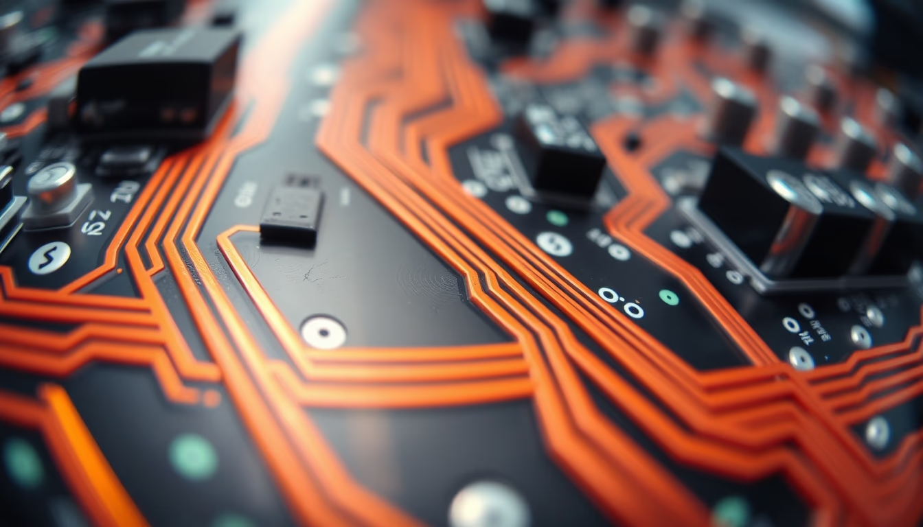
Copper traces on a printed circuit board (PCB) conduct electrical signals between components, essential for electronic device operation.
About this subject
Circuit traces are the thin copper conductive lines that form printed circuit boards (PCBs). They replace traditional wiring, enabling precise and miniaturized connections between components like resistors, capacitors, and chips. The manufacturing process starts with a fiberglass sheet coated with a thin layer of copper. A photosensitive mask is applied and exposed to UV light through a photolithographic film with the circuit design. Unexposed areas are removed chemically, and unprotected copper is etched away by acid solutions, leaving only the desired traces. This method, photolithography followed by chemical etching, achieves high precision, with trace widths on the order of micrometers in modern boards.
PCBs can have single or multiple layers of traces, stacked and separated by dielectric layers. In multilayer boards, traces are interconnected by plated vias, enabling complex circuits in compact spaces, such as smartphones and computers. Copper thickness varies by application: from 18 µm for consumer devices to 70 µm or more for power circuits. Trace width and spacing are critical to prevent shorts and control impedance, especially in high-frequency circuits like 5G antennas. Copper is standard for its excellent conductivity but may be plated with gold or tin to prevent oxidation and improve solderability.
The evolution of circuit traces follows Moore's law, with increasing densities. Techniques like HDI (High Density Interconnect) allow traces as narrow as 50 µm, essential for wearables and IoT devices. Despite sophistication, the basic principle remains since Paul Eisler invented the PCB in the 1940s: creating reliable conductive paths on an insulating substrate. Without these traces, modern electronics, from home appliances to satellites, would not exist.
Frequently Asked Questions
What are circuit traces on a printed circuit board?
They are thin copper lines that connect different electronic components on the board, carrying electrical signals and power. They replace conventional wires and are created by a chemical etching process.
How are circuit traces manufactured?
The process uses photolithography: a copper layer is coated with photoresist, exposed to UV light through a photomask, and unprotected copper is etched away chemically, leaving only the desired traces.
What is the typical thickness of copper traces?
It varies by application: 18 µm (0.5 oz/ft²) for consumer devices, 35 µm (1 oz/ft²) for general use, and up to 105 µm for power circuits. Trace width can be as low as 50 µm in HDI boards.
Direct URL
https://pub-c7d6a6ea828543ac903a74a341ccb2e1.r2.dev/imagens/circuit-traces-pcb-closeup-fish-eye-wide-angle-p7.avifHow to credit
Include a visible link back to UtilizAí. Copy one of the snippets below:
<a href="https://xn--utiliza-eza.com/en/midia/imagens/circuit-traces-pcb-closeup-fish-eye-wide-angle-p7">Circuit traces pcb closeup</a> by <a href="https://xn--utiliza-eza.com">UtilizAí</a>, licensed under <a href="https://creativecommons.org/licenses/by/4.0/">CC BY 4.0</a>.
[Circuit traces pcb closeup](https://xn--utiliza-eza.com/en/midia/imagens/circuit-traces-pcb-closeup-fish-eye-wide-angle-p7) by [UtilizAí](https://xn--utiliza-eza.com), CC BY 4.0
License: CC-BY-4.0





