Chip die exposed silicon
1344×768 · AVIF · CC BY 4.0
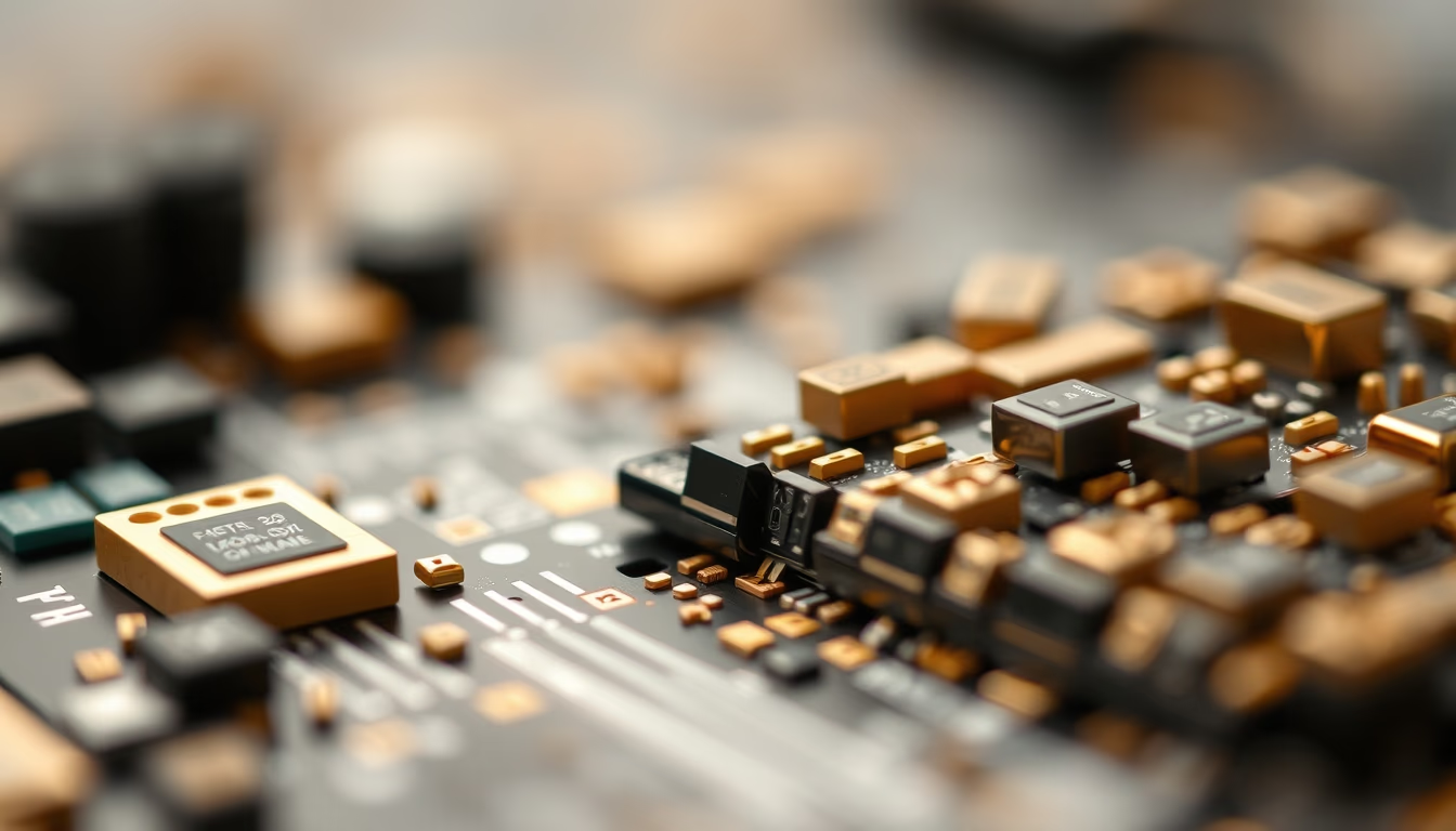
An exposed silicon chip die reveals the heart of microelectronics: a tiny component capable of processing billions of operations per second.
About this subject
A chip die, also known as a silicon die or bare die, is the functional core of any integrated circuit. Fabricated from a monocrystalline silicon wafer, it houses transistors, resistors, and capacitors at nanoscale. After lithography and doping to create conductive regions, the die is separated from the wafer by laser or diamond blade sawing. The tilt-shift effect (simulating shallow depth of field) highlights its geometric structure and the mirror-like surface of exposed silicon.
Silicon is the most widely used semiconductor material due to its abundance, thermal stability, and ability to form an insulating oxide layer (SiO₂). Exposing the silicon on the die enables electrical contact through small metal pads, typically aluminum or copper, which are later bonded to package pins. Each die can contain millions or billions of transistors, as in modern processors and memories.
Manufacturing a die involves hundreds of steps, including cleaning, oxidation, photolithography, etching, and thin-film deposition. Precision is so high that tolerances are measured in nanometers. After electrical testing, known-good dies are assembled into plastic or ceramic packages. Exposed dies (unpackaged) are used in high-power applications or reverse engineering experiments.
Notably, the largest dies on the market belong to GPUs and AI accelerators, such as the NVIDIA GH100 with about 814 mm² area and billions of transistors. The smallest, like RFID chip dies, are less than 1 mm².
Frequently Asked Questions
What is a chip die?
A chip die is the rectangular or square semiconductor block containing the actual integrated circuit, before encapsulation. It is cut from a silicon wafer and houses all transistors and interconnections of the chip.
Why is silicon exposed in some chips?
Chips with exposed silicon are typically bare dies used in special assemblies such as power modules, hybrid circuits, or for direct thermal dissipation. Exposure allows better electrical and thermal contact.
How important is silicon in chip manufacturing?
Silicon is an abundant, low-cost semiconductor that can be doped to create P and N regions. Its native oxide layer (SiO₂) serves as a perfect insulator, essential for the operation of MOS transistors.
Direct URL
https://pub-c7d6a6ea828543ac903a74a341ccb2e1.r2.dev/imagens/chip-die-exposed-silicon-tilt-shift-miniature-p10.avifHow to credit
Include a visible link back to UtilizAí. Copy one of the snippets below:
<a href="https://xn--utiliza-eza.com/en/midia/imagens/chip-die-exposed-silicon-tilt-shift-miniature-p10">Chip die exposed silicon</a> by <a href="https://xn--utiliza-eza.com">UtilizAí</a>, licensed under <a href="https://creativecommons.org/licenses/by/4.0/">CC BY 4.0</a>.
[Chip die exposed silicon](https://xn--utiliza-eza.com/en/midia/imagens/chip-die-exposed-silicon-tilt-shift-miniature-p10) by [UtilizAí](https://xn--utiliza-eza.com), CC BY 4.0
License: CC-BY-4.0





