Chip die exposed silicon
1344×768 · AVIF · CC BY 4.0
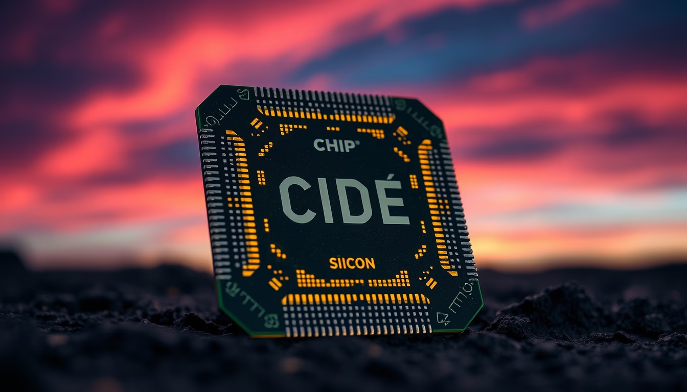
The exposed chip die reveals the internal silicon structure, the core of modern integrated circuits, manufactured in nanoscale processes.
About this subject
The chip die is the silicon substrate containing the integrated circuits (ICs) of a microprocessor or other semiconductor device. It is the functional part of the chip before being encapsulated in a protective package. Manufacturing begins with a monocrystalline silicon wafer, which undergoes lithography and doping processes to create transistors and interconnects at nanometer scale, typically between 5 nm and 14 nm in current chips. This technology is the foundation of CPUs in computers, smartphones, and embedded systems.
Exposing the die is common in reverse engineering, quality control, and hardware photography (such as the long exposure technique used in this image). The die surface usually displays complex geometric patterns resulting from metal and oxide layers. Each chip can contain billions of transistors, as in Apple M1 or Intel Core i9 processors. Production takes place in semiconductor fabs (factories) like those of TSMC, Samsung, and Intel, mainly located in Taiwan, South Korea, and the United States.
Historically, the first integrated circuit was created by Jack Kilby in 1958. Since then, transistor density has doubled roughly every two years (Moore's Law). Today, chips like the NVIDIA H100 have over 80 billion transistors. Die exposure allows detection of manufacturing defects such as particles or cracks, critical for reliability. Long exposure photography enhances surface details and reflected lighting, but the scientific content remains the same: ultra-pure silicon structured for computation.
Fun fact: the silicon used in chip fabrication is one of the purest materials on Earth, with impurities at the parts-per-billion level. The crystal growth process (Czochralski method) produces cylindrical ingots that are cut into wafers. Each wafer goes through hundreds of steps, including extreme ultraviolet (EUV) lithography, to create patterns only a few nanometers wide. The exposed chip die is thus the essence of microelectronics and a testament to precision engineering.
Frequently Asked Questions
What is a chip die?
A chip die is the silicon substrate that contains the integrated circuits of a semiconductor device. It is the functional part before packaging, where transistors and interconnects are etched at nanometer scale.
Why is die exposure important?
Die exposure allows visual inspection for defects, reverse engineering analysis, and photographic documentation. In hardware photography, techniques like long exposure reveal fine surface details of the silicon.
How is a chip die manufactured?
It starts with a monocrystalline silicon wafer. Photolithography, doping, and deposition processes create layers of transistors and metals. Manufacturing occurs in fabs with extreme ultraviolet (EUV) equipment for nanometer-scale patterns.
Direct URL
https://pub-c7d6a6ea828543ac903a74a341ccb2e1.r2.dev/imagens/chip-die-exposed-silicon-long-exposure-p7.avifHow to credit
Include a visible link back to UtilizAí. Copy one of the snippets below:
<a href="https://xn--utiliza-eza.com/en/midia/imagens/chip-die-exposed-silicon-long-exposure-p7">Chip die exposed silicon</a> by <a href="https://xn--utiliza-eza.com">UtilizAí</a>, licensed under <a href="https://creativecommons.org/licenses/by/4.0/">CC BY 4.0</a>.
[Chip die exposed silicon](https://xn--utiliza-eza.com/en/midia/imagens/chip-die-exposed-silicon-long-exposure-p7) by [UtilizAí](https://xn--utiliza-eza.com), CC BY 4.0
License: CC-BY-4.0





