Chip die exposed silicon
1344×768 · AVIF · CC BY 4.0
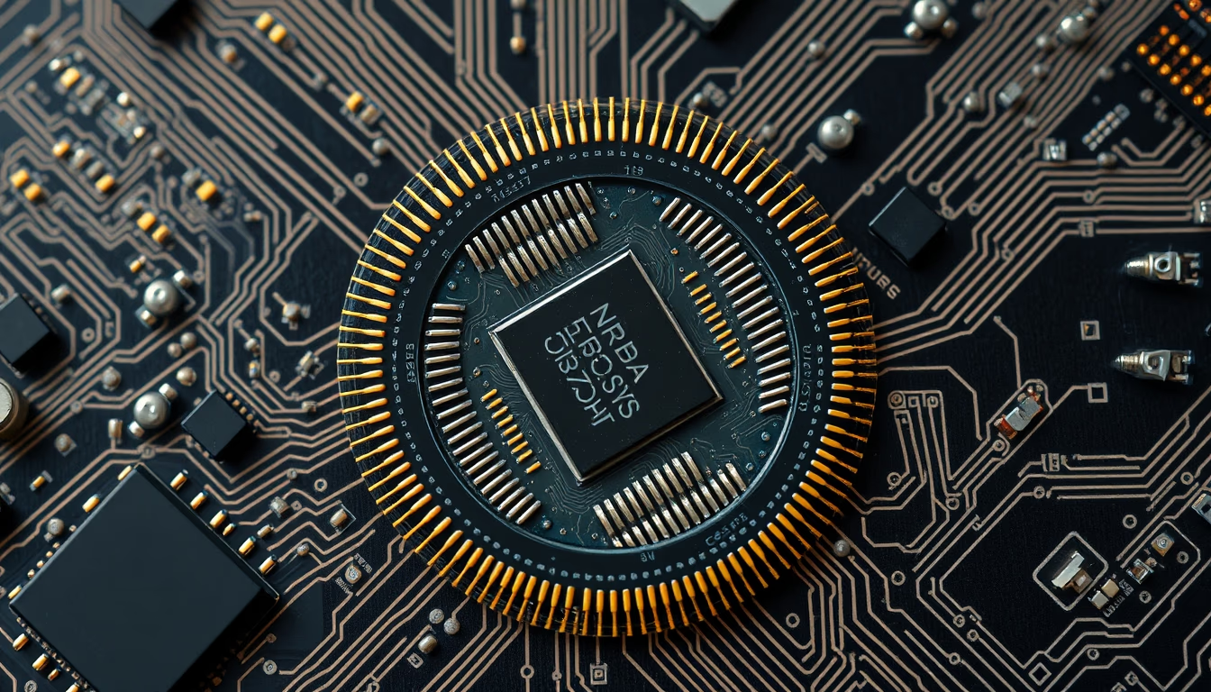
Exposed silicon of a chip die, revealing the intricate integrated circuits that form the foundation of modern electronics.
About this subject
A chip die is the central piece of any integrated circuit, a small silicon substrate where all electronic components, transistors, resistors, capacitors, are fabricated. Silicon is the most widely used semiconductor material due to its abundance and stable electrical properties. Exposing the die reveals the metal and oxide layers forming the intricate interconnections, resulting in a complex geometric pattern.
The manufacturing of a chip die starts with a monocrystalline silicon wafer, cut from a cylindrical ingot. Successive layers of conductive and insulating materials are applied, lithographically patterned, and etched to create millions or billions of transistors. This process, called photolithography, requires Class 1 cleanrooms where particles are nearly absent. With each new technology node, transistors shrink, following Moore's Law, which predicts doubling of transistor density every two years.
Chip dies are separated from the wafer by sawing or laser cutting and encapsulated in protective packages. However, for reverse engineering or quality inspection, the encapsulation is removed chemically or mechanically, exposing the silicon. This practice is common in semiconductor labs to check defects, study competing architectures, or verify design authenticity.
Interestingly, the pattern seen on an exposed die is not random, each rectangular block represents a specific function, such as cache, processing cores, or memory controllers. The bluish or purplish color often results from silicon oxide layers that interfere with light, creating interference effects. These details are crucial for engineers working in microelectronics and chip design.
Frequently Asked Questions
What is a chip die?
A chip die is the silicon substrate containing the integrated circuit of a chip, before packaging. It is the functional part that performs data processing, memory, or other electronic functions.
Why is silicon used in chip manufacturing?
Silicon is an abundant, low-cost semiconductor that forms a stable oxide layer (SiO₂), essential for isolating components. It also supports doping to create P-type and N-type regions, enabling transistors.
How is a chip die exposed?
Exposure typically involves removing the plastic or ceramic encapsulation using acids (like nitric acid) or mechanical methods. The die is then cleaned and photographed under a microscope for analysis.
Direct URL
https://pub-c7d6a6ea828543ac903a74a341ccb2e1.r2.dev/imagens/chip-die-exposed-silicon-isometric-flat-lay-p8.avifHow to credit
Include a visible link back to UtilizAí. Copy one of the snippets below:
<a href="https://xn--utiliza-eza.com/en/midia/imagens/chip-die-exposed-silicon-isometric-flat-lay-p8">Chip die exposed silicon</a> by <a href="https://xn--utiliza-eza.com">UtilizAí</a>, licensed under <a href="https://creativecommons.org/licenses/by/4.0/">CC BY 4.0</a>.
[Chip die exposed silicon](https://xn--utiliza-eza.com/en/midia/imagens/chip-die-exposed-silicon-isometric-flat-lay-p8) by [UtilizAí](https://xn--utiliza-eza.com), CC BY 4.0
License: CC-BY-4.0





