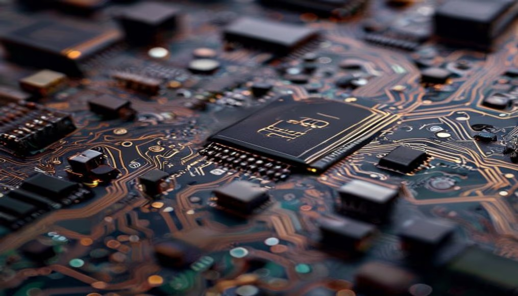
Circuit board macro photography
1344×768 · AVIF · CC BY 4.0

Macro photography of a printed circuit board reveals microscopic details of traces, components, and solder joints.
About this subject
Printed circuit boards (PCBs) form the backbone of virtually all modern electronic devices, from smartphones to satellites. Macro photography of a PCB reveals the complexity of its design: thin copper traces connecting components like resistors, capacitors, and microchips. These traces are chemically etched or mechanically milled onto an insulating substrate, usually fiberglass coated with epoxy resin.
The layout of traces follows strict engineering rules to avoid electromagnetic interference and ensure signal integrity. In multilayer boards, which can have up to 20 layers, connections between layers are made by microvias, tiny plated holes. Macro photography highlights the precision required for mounting SMD (Surface Mount Device) components, which can be as small as 0.4 mm x 0.2 mm.
Interestingly, the common green color of PCBs comes from the solder mask, which protects traces from oxidation and short circuits. Other colors like blue, red, or black are used in consumer or military products for identification or aesthetics. Macro photography also reveals manufacturing marks such as logos and production dates, helping trace the board's origin.
In industrial contexts, visual inspection of PCBs is crucial for quality control. Computer vision machines use macro cameras to detect defects like solder bridges, open traces, or misplaced components. A macro image of a PCB is not only aesthetically interesting but also an engineering and manufacturing tool.
Frequently Asked Questions
What is a printed circuit board (PCB)?
It is a board that connects electronic components using conductive traces, usually copper, on an insulating substrate. It serves as the foundation for electronic circuits.
Why are circuit boards green?
The green color comes from the solder mask, a protective layer that prevents oxidation and shorts. It is the standard color for historical and cost reasons, but other colors exist.
Why is macro photography of PCBs important?
It allows inspection of tiny details like solder joints and traces, essential for quality control in manufacturing and technical documentation.
Direct URL
https://pub-c7d6a6ea828543ac903a74a341ccb2e1.r2.dev/imagens/circuit-board-macro-photography-studio-editorial-portrait-v3.avifHow to credit
Include a visible link back to UtilizAí. Copy one of the snippets below:
<a href="https://xn--utiliza-eza.com/en/midia/imagens/circuit-board-macro-photography-studio-editorial-portrait-v3">Circuit board macro photography</a> by <a href="https://xn--utiliza-eza.com">UtilizAí</a>, licensed under <a href="https://creativecommons.org/licenses/by/4.0/">CC BY 4.0</a>.
[Circuit board macro photography](https://xn--utiliza-eza.com/en/midia/imagens/circuit-board-macro-photography-studio-editorial-portrait-v3) by [UtilizAí](https://xn--utiliza-eza.com), CC BY 4.0
License: CC-BY-4.0