Circuit traces pcb closeup
1344×768 · AVIF · CC BY 4.0
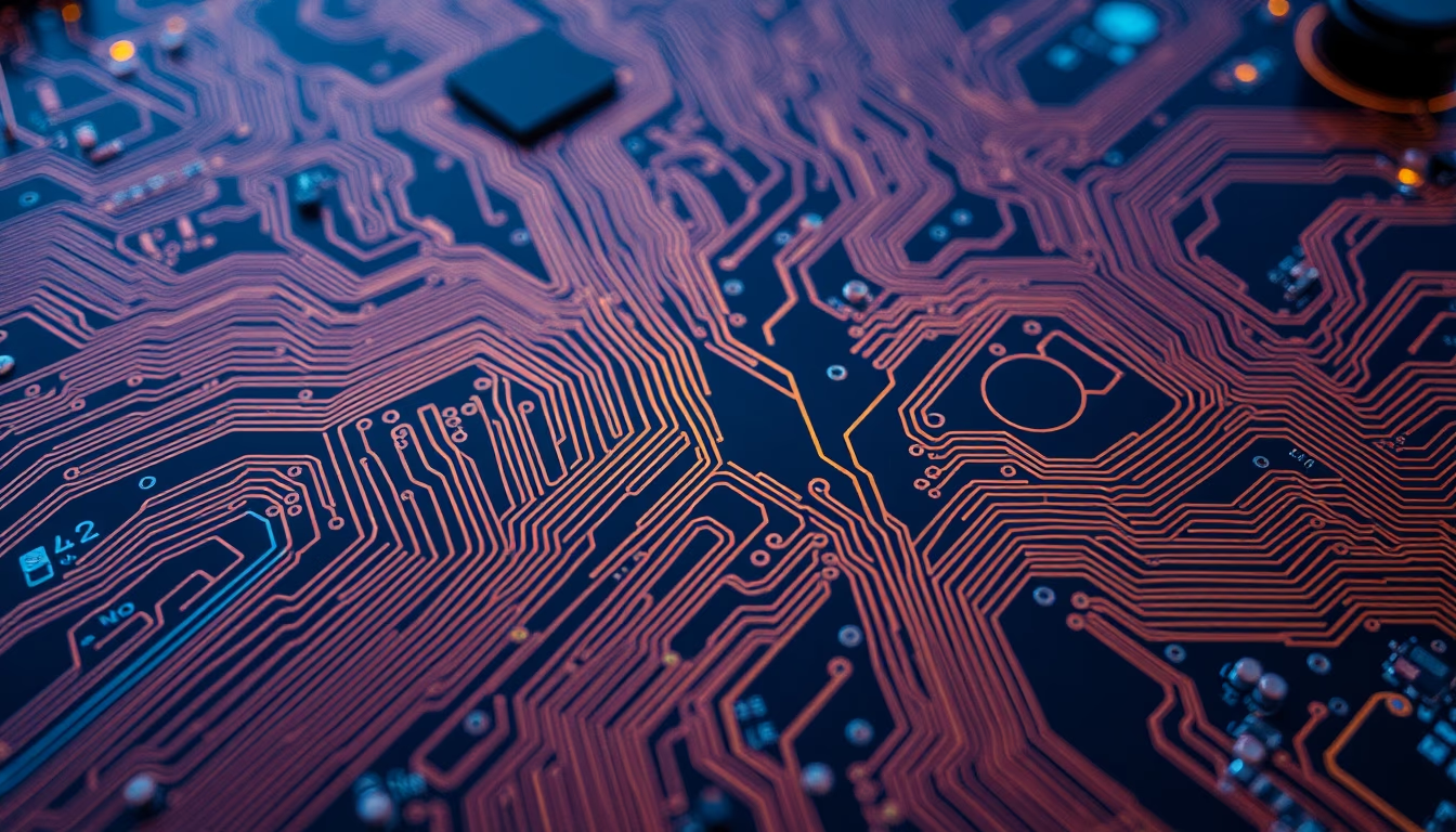
Copper traces on a printed circuit board (PCB), the foundation of modern electronic devices. Understand their function and manufacturing.
About this subject
A printed circuit board (PCB) is the physical support that interconnects electronic components through conductive traces, usually made of copper. These traces are chemically etched or milled onto an insulating base, such as fiberglass or epoxy resin. The manufacturing process begins with laminating a copper foil onto the substrate, followed by applying a photoresist and exposing it to ultraviolet light to define the circuit pattern. After development, the unprotected copper is removed by chemical etching (corrosion), leaving only the desired traces.
PCBs are classified by number of layers: single-sided (one copper layer), double-sided (two layers), or multilayer (several stacked layers, common in complex devices such as smartphones and computers). Each layer is interconnected by plated holes called vias. Typical trace thickness ranges from 0.1 mm to 0.5 mm, depending on the current they must carry. Trace quality is critical to avoid shorts and ensure signal integrity, especially at high frequencies.
PCB manufacturing follows international standards such as IPC (Association Connecting Electronics Industries), which define tolerances for trace width, spacing, and hole diameter. In Brazil, the electronics sector produces about 500,000 square meters of PCBs per year, with emphasis on the Manaus and São Paulo regions. Advanced boards use high-temperature materials or rigid-flex combinations, merging rigid and flexible sections in the same circuit.
Interesting fact: the first PCBs appeared in the 1930s, but only in the 1950s did they become popular with the development of the ferric chloride etching process. Today, almost every electronic device contains at least one PCB, from toys to satellites.
Frequently Asked Questions
What are the copper traces on a circuit board?
Copper traces are conductive pathways etched onto a printed circuit board (PCB) that electrically connect electronic components. They replace wires and cables, enabling compact and reliable circuits.
How is a printed circuit board manufactured?
Manufacturing involves laminating copper onto a substrate, applying photoresist, exposing to UV light with the circuit pattern, developing, and etching away excess copper. The process can produce single or multilayer PCBs with plated holes for interconnection.
What are the main uses of PCBs?
PCBs are used in virtually all electronic devices: smartphones, computers, home appliances, medical equipment, automobiles, and industrial systems. They are essential for miniaturization and circuit reliability.
Direct URL
https://pub-c7d6a6ea828543ac903a74a341ccb2e1.r2.dev/imagens/circuit-traces-pcb-closeup-aerial-drone-shot-p12.avifHow to credit
Include a visible link back to UtilizAí. Copy one of the snippets below:
<a href="https://xn--utiliza-eza.com/en/midia/imagens/circuit-traces-pcb-closeup-aerial-drone-shot-p12">Circuit traces pcb closeup</a> by <a href="https://xn--utiliza-eza.com">UtilizAí</a>, licensed under <a href="https://creativecommons.org/licenses/by/4.0/">CC BY 4.0</a>.
[Circuit traces pcb closeup](https://xn--utiliza-eza.com/en/midia/imagens/circuit-traces-pcb-closeup-aerial-drone-shot-p12) by [UtilizAí](https://xn--utiliza-eza.com), CC BY 4.0
License: CC-BY-4.0





